Updated: AMD Announces Radeon Pro SSG: Fiji With M.2 SSDs On-Board
by Ryan Smith on July 25, 2016 10:30 PM EST- Posted in
- GPUs
- SSDs
- AMD
- Radeon
- Radeon Technologies Group
- Radeon Pro
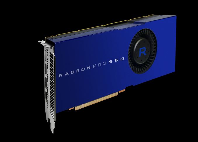
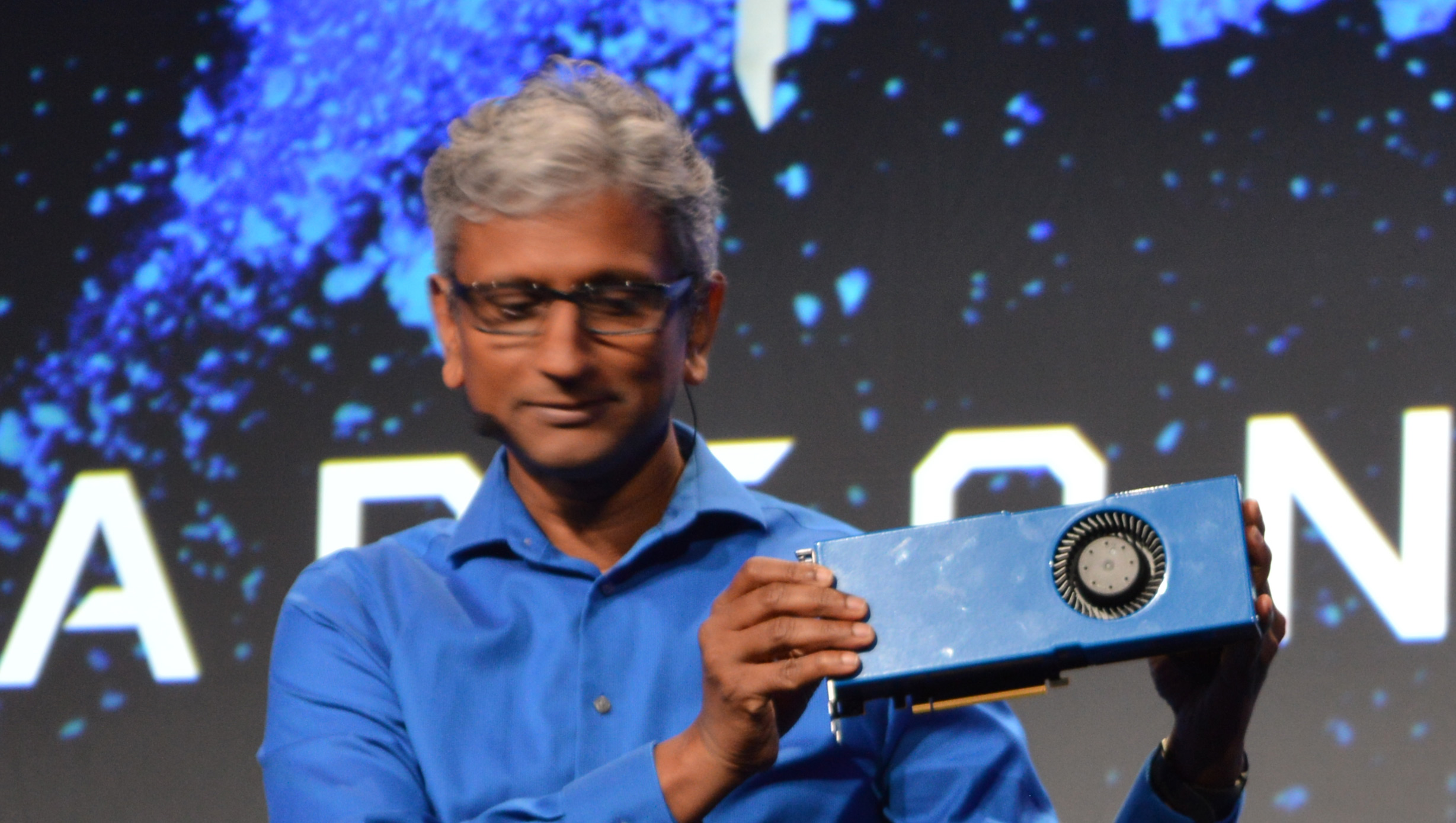
As part of this evening’s AMD Capsaicin event (more on that later), AMD’s Chief Architect and SVP of the Radeon Technologies Group has announced a new Radeon Pro card unlike anything else. Dubbed the Radeon Pro Solid State Graphics (SSG), this card includes M.2 slots for adding NAND SSDs, with the goal of vastly increasing the amount of local storage available to the video card.
Details are a bit thin and I’ll update this later this evening, but in short the card utilizes a Polaris 10 Fiji GPU and includes 2 PCIe 3.0 M.2 slots for adding flash drives to the card. These slots are then attached to the GPU (it’s unclear if there’s a PCIe switch involved or if it’s wired directly), which the GPU can then use as an additional tier of storage. I’m told that the card can fit at least 1TB of NAND – likely limited by M.2 MLC SSD capacities – which massively increases the amount of local storage available on the card.
As AMD explains it, the purpose of going this route is to offer another solution to the workset size limitations of current professional graphics cards. Even AMD’s largest card currently tops out at 32GB, and while this is a fair amount, there are workloads that can use more. This is particular the case for workloads with massive datasets (oil & gas), or as AMD demonstrated, scrubbing through an 8K video file.
Current cards can spill over to system memory, and while the PCIe bus is fast, it’s still much slower than local memory, plus it is subject to the latency of the relatively long trip and waiting on the CPU to address requests. Local NAND storage, by comparison, offers much faster round trips, though on paper the bandwidth isn’t as good, so I’m curious to see just how it compares to the real world datasets that spill over to system memory. Meanwhile actual memory management/usage/tiering is handled by a combination of the drivers and developer software, so developers will need to code specifically for it as things stand.
For the moment, AMD is treating the Radeon Pro SSG as a beta product, and will be selling developer kits for it directly., with full availability set for 2017. For now developers need to apply for a kit from AMD, and I’m told the first kits are available immediately. Interested developers will need to have saved up their pennies though: a dev kit will set you back $9,999.
Update:
Now that AMD’s presentation is over, we have a bit more information on the Radeon Pro SSG and how it works.
In terms of hardware, the Fiji based card is outfit with a PCIe bridge chip – the same PEX8747 bridge chip used on the Radeon Pro Duo, I’m told – with the bridge connecting the two PCIe x4 M.2 slots to the GPU, and allowing both cards to share the PCIe system connection. Architecturally the prototype card is essentially a PCIe SSD adapter and a video card on a single board, with no special connectivity in use beyond what the PCIe bridge chip provides.
The SSDs themselves are a pair of 512GB Samsung 950 Pros, which are about the fastest thing available on the market today. These SSDs are operating in RAID-0 (striped) mode to provide the maximum amount of bandwidth. Meanwhile it turns out that due to how the card is configured, the OS actually sees the SSD RAID-0 array as well, at least for the prototype design.
To use the SSDs, applications need to be programmed using AMD’s APIs to recognize the existence of the local storage and that it is “special,” being on the same board as the GPU itself. Ultimately the trick for application developers is directly streaming resources from the SSDs treating it as a level of cache between the DRAM and system storage. The use of NAND in this manner does not fit into the traditional memory hierarchy very well, as while the SSDs are fast, on paper accessing system memory is faster still. But it should be faster than accessing system storage, even if it’s PCIe SSD storage elsewhere on the system. Similarly, don’t expect to see frame buffers spilling over to NAND any time soon. This is about getting large, mostly static resources closer to the GPU for more efficient resource streaming.
To showcase the potential benefits of this solution, AMD had an 8K video scrubbing demonstration going, comparing performance between using a source file on the SSG’s local SSDs, and using a source file on the system SSD (also a 950 Pro).
See what the Radeon™ Pro SSG can do to help drastically improve professional workload enablement #AMDCapsaicinhttps://t.co/ZkcfffSScN
— Radeon Pro (@RadeonPro) July 26, 2016
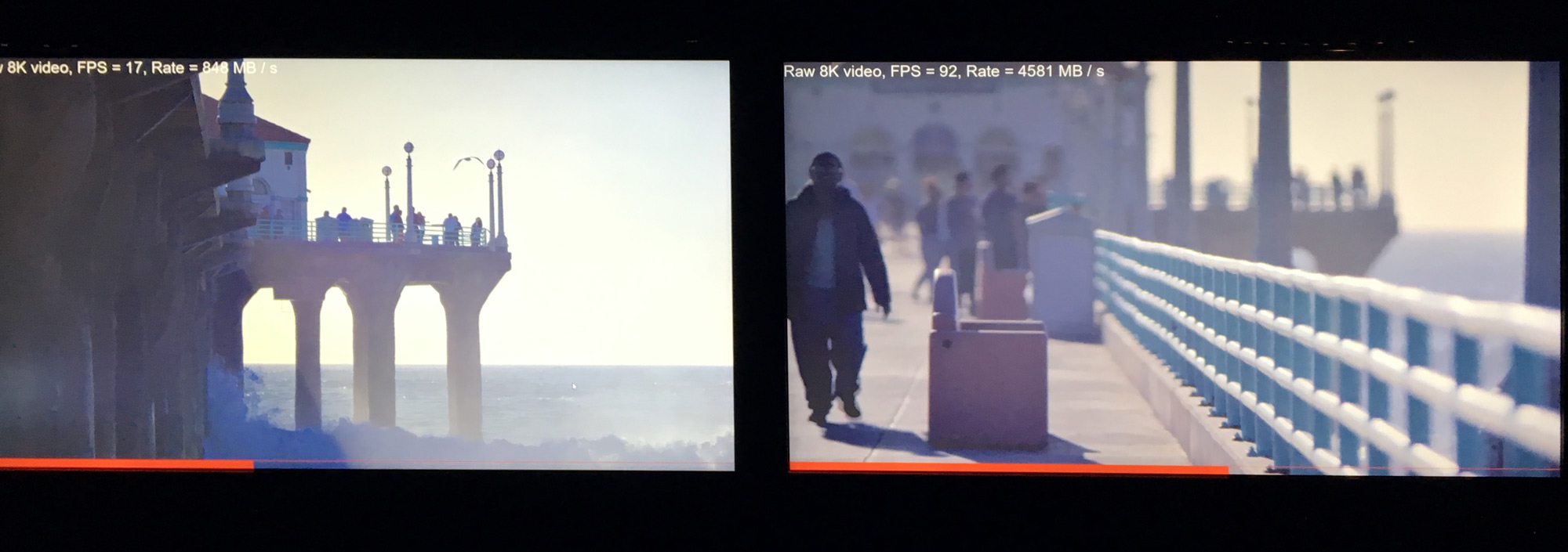
The performance differential was actually more than I expected; reading a file from the SSG SSD array was over 4GB/sec, while reading that same file from the system SSD was only averaging under 900MB/sec, which is lower than what we know 950 Pro can do in sequential reads. After putting some thought into it, I think AMD has hit upon the fact that most M.2 slots on motherboards are routed through the system chipset rather than being directly attached to the CPU. This not only adds another hop of latency, but it means crossing the relatively narrow DMI 3.0 (~PCIe 3.0 x4) link that is shared with everything else attached to the chipset.
Though by and large this is all at the proof of concept stage. The prototype, though impressive in some ways in its own right, is really just a means to get developers thinking about the idea and writing their applications to be aware of the local storage. And this includes not just what content to put on the SSG's SSDs, but also how to best exploit the non-volatile nature of its storage, and how to avoid unnecessary thrashing of the SSDs and burning valuable program/erase cycles. The SSG serves an interesting niche, albeit a limited one: scenarios where you have a large dataset and you are somewhat sensitive to latency and want to stay off of the PCIe bus, but don't need more than 4-5GB/sec of read bandwidth. So it'll be worth keeping an eye on this to see what developers can do with it.
In any case, while AMD is selling dev kits now, expect some significant changes by the time we see the retail hardware in 2017. Given the timeframe I expect we’ll be looking at much more powerful Vega cards, where the overall GPU performance will be much greater, and the difference in performance between memory/storage tiers is even more pronounced.
Source: AMD


120 Comments
View All Comments
vladx - Tuesday, July 26, 2016 - link
Few thousand? If they manage to sell 100 of these, AMD will consider themselves "lucky".FMinus - Tuesday, July 26, 2016 - link
A university here runs around ~650 FirePRO W9100 alone, what makes you think they only sell low volume of those cards, aside from your stupidity.vladx - Tuesday, July 26, 2016 - link
Because the price is 10k/piece and the use cases are much smaller than an ordinary workstation card.vladx - Tuesday, July 26, 2016 - link
No university in the world will buy such an esoteric solutions.silverblue - Tuesday, July 26, 2016 - link
No, the dev kit is $10K, but I suppose that won't stop AMD charging a lot if it has customers who will pay it.vladx - Tuesday, July 26, 2016 - link
I was only refering to the developer kit obviously since that's the only price we got, duh.eachus - Sunday, July 31, 2016 - link
Ever heard of the Large Synoptic Survey Telescope? https://www.lsst.org/ These cards will be very useful for building up a base image of the sky, and noting changes with each image. One problem, since the telescope has a 3200 megapixel CCD, it would take 32 or more of these, in separate workstations. Not a problem really, dozens of astronomers will chose sectors of the images to work with. The number of "events" to process, per image, will be in the thousands.But to me, the real use case is sesmic processing. You spend hours, often days of supercomputer time coming up with one three dimensional image, several gigabytes in size. Then an analyst downloads the image to a workstation, and tries to make sense of it. The pretty sesmic images you may have seen, are pretty, but are also the result of hours of post-processing by a skilled analyst to create an image which is easy to read. Having the data local, rather than supplied by a server, will take lots of coffee breaks out of the process. (Points where you wait three or four minutes for the next image to be created.)
D. Lister - Monday, July 25, 2016 - link
"Meanwhile actual memory management/usage/tiering is handled by a combination of the drivers and developer software, so developers will need to code specifically for it as things stand."...and all the developers need to do, before they specifically code for this one product, is to pay a paltry $10,000, and hope that this is indeed a real product, that will have long enough support and supply by AMD for it to be worth the developes' work and expense. Yeah, sounds like a winning idea already. If they kept clutching at straws like this, I might start thinking they may be drowning or something.
rhysiam - Monday, July 25, 2016 - link
I'm confused. Surely even on-card PCIe NVMe drives are going to be substantially slower and higher latency than going to system RAM. So in any cases where system RAM can act as the buffer, this solution loses.Then if you really need a larger buffer than system ram can provide, is going via the system actually such a significant bottleneck that an onboard NVMe drive over a system one makes a sizeable difference? Even a local drive will have a PCIe interface to navigate as well as the latency inherent in reading the flash. So we're already into the hundreds of microseconds territory. Does a system M.2 NVMe drive actually add that much more?
I'm guessing the answer is "yes", or this would be utterly pointless. Am I missing something?
jjj - Tuesday, July 26, 2016 - link
Could be designed for xpoint and then, we don't have the data for xpoint to speculate.