AMD 7th Gen Bristol Ridge and AM4 Analysis: Up to A12-9800, B350/A320 Chipset, OEMs first, PIBs Later
by Ian Cutress on September 23, 2016 9:00 AM ESTUnderstanding Connectivity: Some on the APU, External Chipset Optional
Users keeping tabs on the developments of CPUs will have seen the shift over the last ten years to moving the traditional ‘northbridge’ onto the main CPU die. The northbridge was typically the connectivity hub, allowing the CPU to communicate to the PCIe, DRAM and the Chipset (or Southbridge), and moving this onto the CPU silicon gave better latency, better power characteristics, and reduced the complexity of the motherboard, all for a little extra die area. Typically when we say ‘CPU’ in the context of a modern PC build, this is the image we have, with the CPU containing cores and possibly graphics (which AMD calls an APU).
Typically the CPU/APU has limited connectivity: video outputs (if an integrated GPU is present), a PCIe root complex for the main PCIe lanes, and an additional connectivity pathway to the chipset to enable additional input/output functionality. The chipset uses a one-to-many philosophy, whereby the total bandwidth between the CPU and Chipset may be lower than the total bandwidth of all the functionality coming out of the chipset. Using FIFO buffers, this is typically managed as required. The best analogy for this is that a motorway is not 50 million lanes wide, because not all cars use it at the same time. You only need a few lanes to cater for all but the busiest circumstances.
If the CPU also has the chipset/southbridge built in, either in the silicon or as a multi-chip package, we typically call this an ‘SoC’, or system on chip, as the one unit has all the connectivity needed to fully enable its use. Add on some slots, some power delivery and firmware, then away you go.
Bristol Ridge’s ‘SoC’ Configuration
What AMD is doing with Bristol Ridge is a half-way house between a SoC and having a fully external chipset. Some of the connectivity, such as SATA ports, PCIe storage, or PCIe lanes beyond the standard GPU lanes, is built into the processor. These fall under the features of the processor, and for the current launch is a fixed set of features. The CPU also has additional connectivity to an optional chipset which can provide more features, however the use of the chipset is optional.
Here’s a block diagram to help explain:
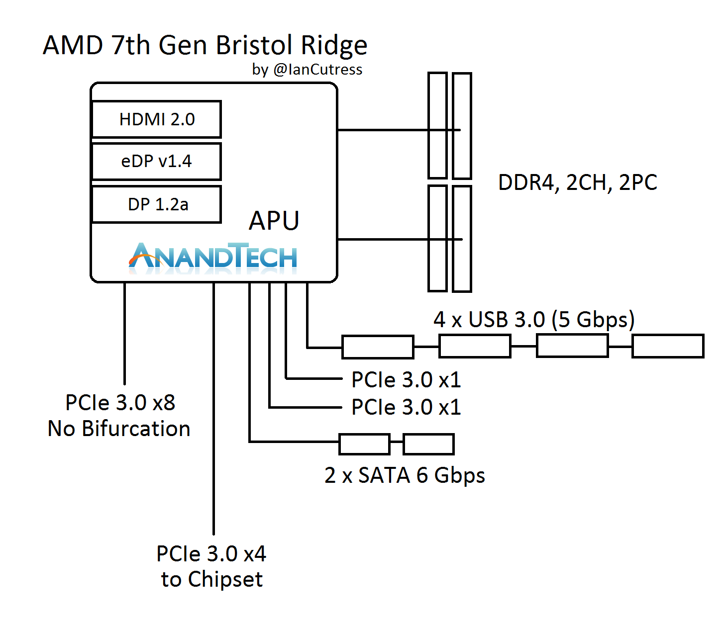
On the APU we have two channels of DDR4, supporting two DIMMs per channel. For the major PCIe devices, we have a PCIe 3.0 x8 port, and this does not support bifurcation (or splitting) to any x4, x2 or x1 combination. It’s a solitary x8 lane suitable for a PCIe x8 port (we’ll discuss what else can be done with this later). The APU communicates with the optional chipset with a PCIe 3.0 x4 link, and we’ve confirmed with AMD that this is a simple PCIe interface. The other parts of the APU give four USB 3.0 ports, two SATA 6 Gbps ports, and two PCIe 3.0 x1 ports. These ports also support NVMe, and can provide two PCIe 3.0 x1 storage ports or can be combined for a single PCIe 3.0 x2.
It Looks Like an x16
Now, if you look at the layout, try counting up how many PCIe lanes are split across all the features. We’ve seen a USB 3.0 hub support four ports of USB 3.0 from a single lane of PCIe 3.0 before, and there are plenty of controllers out there that split a PCIe 3.0 x1 into two SATA ports. So play the adding game: x8 + x4 + x1 + x1 + x1 + x1 = x16. The Bristol Ridge APU seems to suggest it actually has sixteen PCIe 3.0 lanes, but AMD has decided to forcibly split some of them using internal hubs and controllers.
It’s an interesting tactic because it means that systems can be built without a discrete chipset, or the four chipset lanes can be used for other features. However it negates a full PCIe 3.0 x16 link for a full-bandwidth PCIe co-processor. Bearing in mind that if there was a PCIe 3.0 x16 link, there are no additional lanes for a chipset, so there would not be any IO such as SATA ports anyway, such that there would be no physical storage.
The x16 total theory is also somewhat backed up by the lack of bifurcation on the x8 link. Historically a PCIe root complex in a consumer platform that supports x16 can be bifurcated down to x8/x4/x4, and anything else requires additional PCIe switches to support more than three devices. It would seem that AMD has taken the final x4 link and added an on-die PCIe switch to provide those ports, for standard PCIe to USB/SATA controllers. I would hazard a guess and say that what AMD has done is more integrated and complicated than this, in order to keep die area low.
PCIe is Fun with Switches: PLX, Thunderbolt, 10GigE, the Kitchen Sink
Another thing about the x8 link is that it can be combined with an external PCIe switch. In my discussions with AMD, they suggested a switch that bifurcates the x8 to dual x4 interfaces, which could leverage fast PCIe storage while maintaining the onboard graphics for any GPU duties. There’s the other side, in using an x8 to x32 PCIe switch and affording two large x16 links. However, large GPU CrossFire is not one of the main aims for the platform.
Here’s a crazy mockup I thought of, using a $100 PCIe switch. I doubt this would come to market.
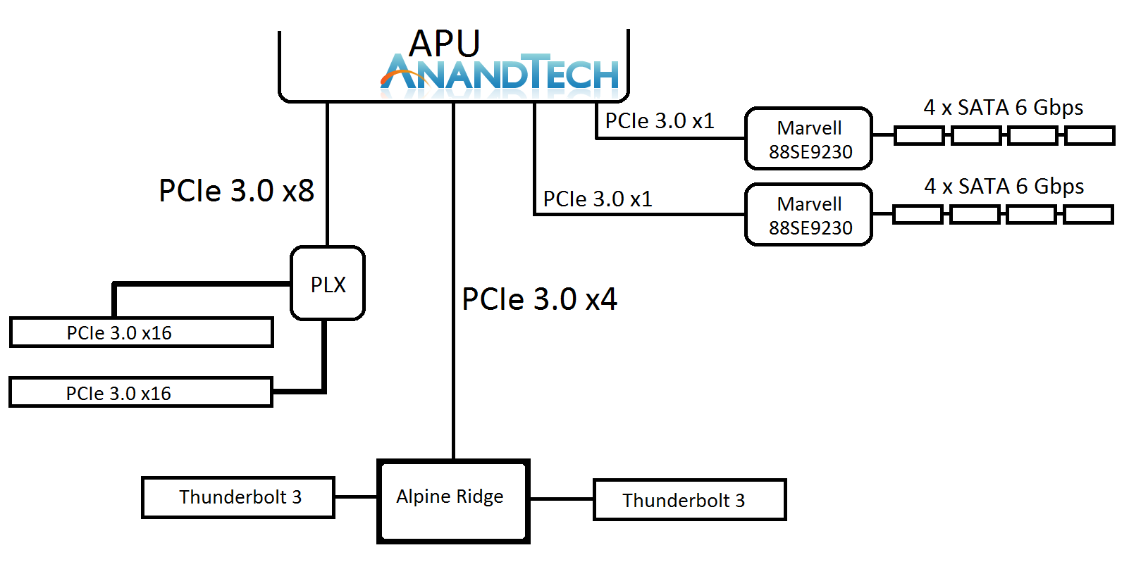
Ian plays a crazy game of PCIe Lego
The joy of PCIe and switches is that it becomes a mix and match game - there’s also the PCIe 3.0 x4 to the chipset. This can be used for non-chipset duties, such as anything that takes PCIe 3.0 x4 like a fast SSD, or potentially Thunderbolt 3. We discussed TB3 support, via Intel’s Alpine Ridge controller, and we were told that the AM4 platform is currently being validated for systems supporting AMD XConnect, which will require Thunderbolt support. AMD did state that they are not willing to speculate on TB3 use, and from my perspective this is because the external GPU feature is what AMD is counting on as being the primary draw for TB3 enabled systems (particularly for OEMs). I suspect the traditional motherboard manufacturers will offer wilder designs, and ASRock likes to throw some spaghetti at the wall, to see what sticks.


122 Comments
View All Comments
ddriver - Saturday, September 24, 2016 - link
Hey, at least Trump is only preposterous and stupid. Hillary is all that PLUS crazy and evil. She is just as racist as Trump, if not more so, but she is not in the habit of being honest, she'd prefer to claim the votes of minorities.Politics is a joke and the current situation is a very good example of it. People deserve all shit that coming their way if they still put faith in the political process after this.
ClockHound - Friday, September 23, 2016 - link
+101Particularly enjoyed the term: "walled garden spyware milking station" model
Ok, not really enjoyed, cringed at the accuracy, however. ;-)
msroadkill612 - Wednesday, April 26, 2017 - link
An adage I liked "If its free, YOU are the product."hoohoo - Friday, September 23, 2016 - link
I see what you did there! Nicely done.patrickjp93 - Saturday, September 24, 2016 - link
No they aren't. If Geekbench optimized for x86 the way it does for ARM, the difference in performance per clock is nearly 5xddriver - Saturday, September 24, 2016 - link
You have no idea what you are talking about. Geekbench is very much optimized, there are basically three types of optimization:optimization done by the compiler - it eliminates redundant code, vertorizes loops and all that good stuff, that happens automatically
optimization by using intrinsics - do manually what the compiler does automatically, sometimes you could do better, but in general, compiler optimizations are very mature and very good at doing what they do
"optimization" of the type "if (CPUID != INTEL) doWorse()" - harmful optimization that doesn't really optimize anything in the true sense of the word, but deliberately chooses a less efficient code path to purposely harm the performance of a competitor - such optimizations are ALWAYS in the favor of the TOP DOG - be that intel or nvidia - companies who have excess of money to spend on such idiotic things. Smaller and less profitable companies like amd or arm - they don't do that kind of shit.
Finally, performance is not magic, you can't "optimize" and suddenly get 5X the performance. Process and TDP are a limiting factor, there is only so much performance you can get out of a chip produced at a given process for a given thermal budget. And that's if it is some perfectly efficient design. A 5W 20nm x86 chip could not possibly be any faster than a 5W 20nm ARM chip, intel has always had a slight edge in process, but if you manufacture an arm and a x86 chip on identical process (not just the claimed node size) with the same thermal budget the amr chip will be a tad faster, because the architecture is less bloated and more efficient.
It is a part of a dummy's belief system that arm chips are somehow fundamentally incapable of running professional software - on the contrary, hardware wise they are perfectly capable, only nobody bothers to write professional software for them.
patrickjp93 - Saturday, September 24, 2016 - link
I have a Bachelor's in computer science and specialized in high performance parallel, vectorized, and heterogeneous computing. I've disassembled Geekbench on x86 platforms, and it doesn't even use anything SSE or higher, and that's ancient Pentium III instructions.It does not happen automatically if you don't use the right compiler flags and don't have your data aligned to allow the instructions to work.
You need intrinsics for a lot of things. Clang and GCC both have huge compiler bug forums filled with examples of where people beat the compilers significantly.
Yes you can get 5x the performance by optimizing. Geekbench only handles 1 datem at a time on Intel hardware vs. the 8 you can do with AVX and AVX2. Assuming you don't choke on bandwidth, you can get an 8x speedup.
ARM is not more efficient on merit, and x86 is not bloated by any stretch. Both use microcode now. ARM is no longer RISC by any strict definition.
Cavium has. Oracle has. Google has. Amazon has. In all cases ARM could not keep up with Avoton and Xeon D in performance/watt/$ and thus the industry stuck with Intel instead of Qualcomm or Cavium.
Toss3 - Sunday, September 25, 2016 - link
This is a great post, and I just wanted to post an article by PC World where they discussed these things in simpler terms: http://www.pcworld.com/article/3006268/tablets/tes...As you can see the performance gains aren't really that great when it comes to real world usage, and as such we should probably start to use other benchmarks as well, and not just use Geekbench or browser javascript performance as indicators of actual performance of these SoCs especially when comparing one platform to another.
amagriva - Sunday, September 25, 2016 - link
Good post. To any interested a good paper on the subject : http://etn.se/images/expert/FD-SOI-eQuad-white-pap...ddriver - Sunday, September 25, 2016 - link
I've been using GCC mostly, and in most of the cases after doing explicit vectorization I found no perf benefits, analyzing assembly afterwards revealed that the compiled has done a very good job at vectorizing wherever possible.However, I am highly skeptical towards your claims, I'll believe it when I see it. I can't find the link now, but last year I've read detailed analysis, showing that A9X core performance per watt better than skylake over most of the A9X's clock range. And not in geekbench, but in SPEC.
As for geekbench, you make it sound as if they actually disabled vectorization explicitly. Which would be an odd thing. Not entirely clear what you mean by "1 datem at a time", but if you mean they are using scalar rather than vector instructions, that would be quite odd too. Luckily, I have better things to do than rummage about in geekbench machine code, so I will take your word that it is not properly optimized.
And sure, 256bit wide SIMD will have higher throughput than 128bit SIMD, but nowhere nearly 8 or even 5 times. And that doesn't make arm chips any less capable of running devices, which are more than useless toys. Those chips are more powerful than workstations were some 10 years ago, but their usability is nowhere near that. As the benchmarks from the link Toss3 posted indicate, the A9X is only some ~40% slower than i5-4300U in the "true/real world benchmarks", and that's a 15 watt chip vs the A9X is like what, 5-ish or something like that? And ARM is definitely more efficient once you account for intel's process advantage. This will become obvious if intel ever dare to manufacture arm cores at the same process as their own products. And it is not because of the ISA bloat but because of the design bloat.
Naturally, ARM chips are a low margin product, one cannot expect a 50$ chip to outperform a 300$ chip, but the gap appears to be closing, especially keeping in mind the brickwall process is going to hit the next decade. A 50$ chip running equal to a 300$ (and much wider design) chip from 2 year ago opens up a lot of possibilities, but I am not seeing any of them being realized by the industry.