AMD 7th Gen Bristol Ridge and AM4 Analysis: Up to A12-9800, B350/A320 Chipset, OEMs first, PIBs Later
by Ian Cutress on September 23, 2016 9:00 AM ESTUnderstanding Connectivity: Some on the APU, External Chipset Optional
Users keeping tabs on the developments of CPUs will have seen the shift over the last ten years to moving the traditional ‘northbridge’ onto the main CPU die. The northbridge was typically the connectivity hub, allowing the CPU to communicate to the PCIe, DRAM and the Chipset (or Southbridge), and moving this onto the CPU silicon gave better latency, better power characteristics, and reduced the complexity of the motherboard, all for a little extra die area. Typically when we say ‘CPU’ in the context of a modern PC build, this is the image we have, with the CPU containing cores and possibly graphics (which AMD calls an APU).
Typically the CPU/APU has limited connectivity: video outputs (if an integrated GPU is present), a PCIe root complex for the main PCIe lanes, and an additional connectivity pathway to the chipset to enable additional input/output functionality. The chipset uses a one-to-many philosophy, whereby the total bandwidth between the CPU and Chipset may be lower than the total bandwidth of all the functionality coming out of the chipset. Using FIFO buffers, this is typically managed as required. The best analogy for this is that a motorway is not 50 million lanes wide, because not all cars use it at the same time. You only need a few lanes to cater for all but the busiest circumstances.
If the CPU also has the chipset/southbridge built in, either in the silicon or as a multi-chip package, we typically call this an ‘SoC’, or system on chip, as the one unit has all the connectivity needed to fully enable its use. Add on some slots, some power delivery and firmware, then away you go.
Bristol Ridge’s ‘SoC’ Configuration
What AMD is doing with Bristol Ridge is a half-way house between a SoC and having a fully external chipset. Some of the connectivity, such as SATA ports, PCIe storage, or PCIe lanes beyond the standard GPU lanes, is built into the processor. These fall under the features of the processor, and for the current launch is a fixed set of features. The CPU also has additional connectivity to an optional chipset which can provide more features, however the use of the chipset is optional.
Here’s a block diagram to help explain:
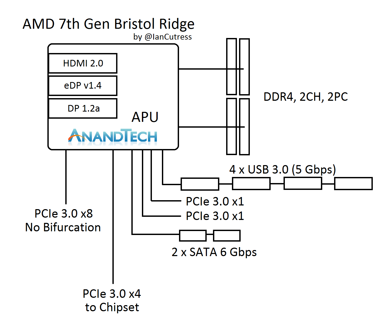
On the APU we have two channels of DDR4, supporting two DIMMs per channel. For the major PCIe devices, we have a PCIe 3.0 x8 port, and this does not support bifurcation (or splitting) to any x4, x2 or x1 combination. It’s a solitary x8 lane suitable for a PCIe x8 port (we’ll discuss what else can be done with this later). The APU communicates with the optional chipset with a PCIe 3.0 x4 link, and we’ve confirmed with AMD that this is a simple PCIe interface. The other parts of the APU give four USB 3.0 ports, two SATA 6 Gbps ports, and two PCIe 3.0 x1 ports. These ports also support NVMe, and can provide two PCIe 3.0 x1 storage ports or can be combined for a single PCIe 3.0 x2.
It Looks Like an x16
Now, if you look at the layout, try counting up how many PCIe lanes are split across all the features. We’ve seen a USB 3.0 hub support four ports of USB 3.0 from a single lane of PCIe 3.0 before, and there are plenty of controllers out there that split a PCIe 3.0 x1 into two SATA ports. So play the adding game: x8 + x4 + x1 + x1 + x1 + x1 = x16. The Bristol Ridge APU seems to suggest it actually has sixteen PCIe 3.0 lanes, but AMD has decided to forcibly split some of them using internal hubs and controllers.
It’s an interesting tactic because it means that systems can be built without a discrete chipset, or the four chipset lanes can be used for other features. However it negates a full PCIe 3.0 x16 link for a full-bandwidth PCIe co-processor. Bearing in mind that if there was a PCIe 3.0 x16 link, there are no additional lanes for a chipset, so there would not be any IO such as SATA ports anyway, such that there would be no physical storage.
The x16 total theory is also somewhat backed up by the lack of bifurcation on the x8 link. Historically a PCIe root complex in a consumer platform that supports x16 can be bifurcated down to x8/x4/x4, and anything else requires additional PCIe switches to support more than three devices. It would seem that AMD has taken the final x4 link and added an on-die PCIe switch to provide those ports, for standard PCIe to USB/SATA controllers. I would hazard a guess and say that what AMD has done is more integrated and complicated than this, in order to keep die area low.
PCIe is Fun with Switches: PLX, Thunderbolt, 10GigE, the Kitchen Sink
Another thing about the x8 link is that it can be combined with an external PCIe switch. In my discussions with AMD, they suggested a switch that bifurcates the x8 to dual x4 interfaces, which could leverage fast PCIe storage while maintaining the onboard graphics for any GPU duties. There’s the other side, in using an x8 to x32 PCIe switch and affording two large x16 links. However, large GPU CrossFire is not one of the main aims for the platform.
Here’s a crazy mockup I thought of, using a $100 PCIe switch. I doubt this would come to market.
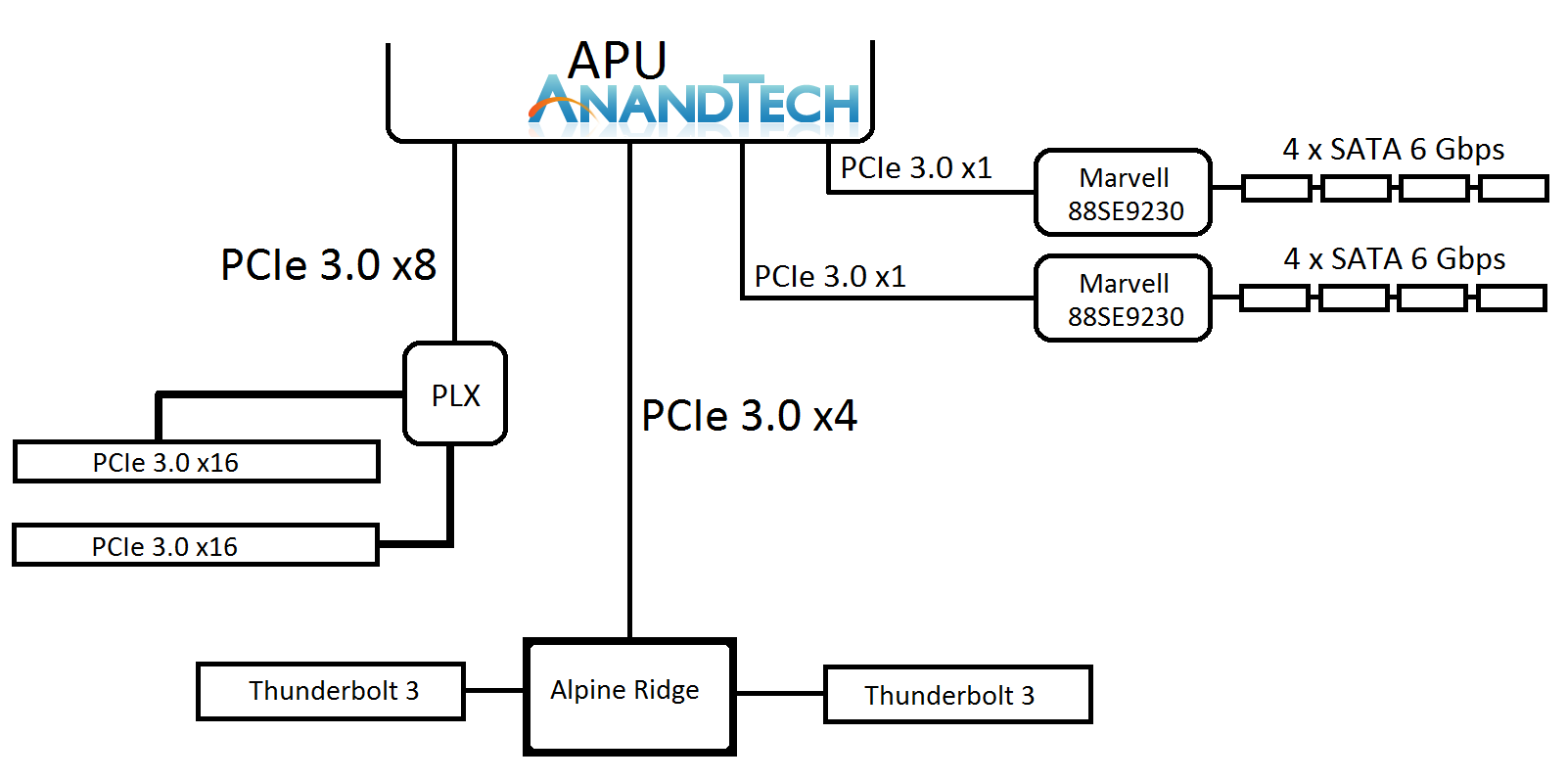
Ian plays a crazy game of PCIe Lego
The joy of PCIe and switches is that it becomes a mix and match game - there’s also the PCIe 3.0 x4 to the chipset. This can be used for non-chipset duties, such as anything that takes PCIe 3.0 x4 like a fast SSD, or potentially Thunderbolt 3. We discussed TB3 support, via Intel’s Alpine Ridge controller, and we were told that the AM4 platform is currently being validated for systems supporting AMD XConnect, which will require Thunderbolt support. AMD did state that they are not willing to speculate on TB3 use, and from my perspective this is because the external GPU feature is what AMD is counting on as being the primary draw for TB3 enabled systems (particularly for OEMs). I suspect the traditional motherboard manufacturers will offer wilder designs, and ASRock likes to throw some spaghetti at the wall, to see what sticks.


122 Comments
View All Comments
Meteor2 - Saturday, September 24, 2016 - link
This. If HSA was *actually used* AMD performance would be fantastic.Shadowmaster625 - Sunday, September 25, 2016 - link
HSA is a pipe dream. Too much latency.patrickjp93 - Monday, September 26, 2016 - link
No it wouldn't. HSA requires code bloat which will damage cache friendliness in all cases where code cannot be offloaded to the iGPU. This is why Oracle, Fujitsu, IBM, Intel, and Nvidia all turned their nose up at it. HPX, OpenMP, and OpenACC kick the snot out of HSA as both a programming model and a hardware interface.Vayra - Friday, September 23, 2016 - link
I don't. Who cares about Apple in any comparison? They walled their garden. You go Apple or you go for something sensible.AbbieHoffman - Friday, November 11, 2016 - link
Why? Apple is just old outdated crap propped up by dumb hollywood trendies that don't know any better. Also Apple basically has slave labor and suicide nets around the buildings that house their employees. They won't even let them escape in death.romrunning - Friday, September 23, 2016 - link
Forget these older designs - let's get Zen released already, and work on a Zen mobile/ULV platform.euskalzabe - Friday, September 23, 2016 - link
Agreed... just release Zen already. I hope at least motherboards will be available by Xmas. Get the build ready, but a Zen CPU in jan/feb, drop it in and boom, new PC build.kn00tcn - Friday, September 23, 2016 - link
how is releasing mobos early any good? what happens if for whatever reason there are problems with old mobos when the high end cpus come (in a way similar to early ddr3 being higher voltage)Murloc - Saturday, September 24, 2016 - link
yeah it's just stupid to buy stuff to have it become old in your house before you can even use itKrysto - Friday, September 23, 2016 - link
Yeah, when can we expect Zen mobile APUs already?