AMD 7th Gen Bristol Ridge and AM4 Analysis: Up to A12-9800, B350/A320 Chipset, OEMs first, PIBs Later
by Ian Cutress on September 23, 2016 9:00 AM ESTUnderstanding Connectivity: Some on the APU, External Chipset Optional
Users keeping tabs on the developments of CPUs will have seen the shift over the last ten years to moving the traditional ‘northbridge’ onto the main CPU die. The northbridge was typically the connectivity hub, allowing the CPU to communicate to the PCIe, DRAM and the Chipset (or Southbridge), and moving this onto the CPU silicon gave better latency, better power characteristics, and reduced the complexity of the motherboard, all for a little extra die area. Typically when we say ‘CPU’ in the context of a modern PC build, this is the image we have, with the CPU containing cores and possibly graphics (which AMD calls an APU).
Typically the CPU/APU has limited connectivity: video outputs (if an integrated GPU is present), a PCIe root complex for the main PCIe lanes, and an additional connectivity pathway to the chipset to enable additional input/output functionality. The chipset uses a one-to-many philosophy, whereby the total bandwidth between the CPU and Chipset may be lower than the total bandwidth of all the functionality coming out of the chipset. Using FIFO buffers, this is typically managed as required. The best analogy for this is that a motorway is not 50 million lanes wide, because not all cars use it at the same time. You only need a few lanes to cater for all but the busiest circumstances.
If the CPU also has the chipset/southbridge built in, either in the silicon or as a multi-chip package, we typically call this an ‘SoC’, or system on chip, as the one unit has all the connectivity needed to fully enable its use. Add on some slots, some power delivery and firmware, then away you go.
Bristol Ridge’s ‘SoC’ Configuration
What AMD is doing with Bristol Ridge is a half-way house between a SoC and having a fully external chipset. Some of the connectivity, such as SATA ports, PCIe storage, or PCIe lanes beyond the standard GPU lanes, is built into the processor. These fall under the features of the processor, and for the current launch is a fixed set of features. The CPU also has additional connectivity to an optional chipset which can provide more features, however the use of the chipset is optional.
Here’s a block diagram to help explain:
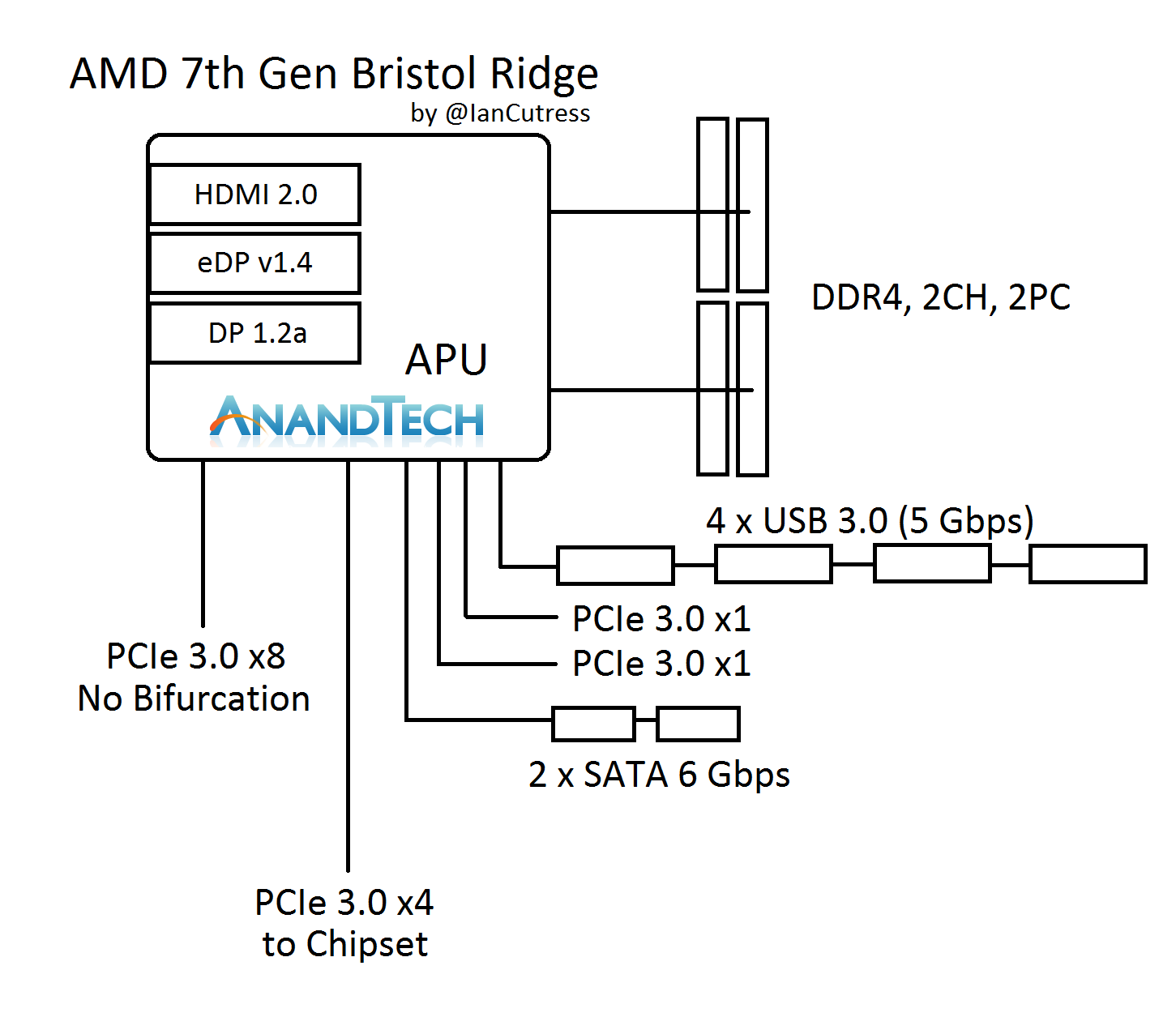
On the APU we have two channels of DDR4, supporting two DIMMs per channel. For the major PCIe devices, we have a PCIe 3.0 x8 port, and this does not support bifurcation (or splitting) to any x4, x2 or x1 combination. It’s a solitary x8 lane suitable for a PCIe x8 port (we’ll discuss what else can be done with this later). The APU communicates with the optional chipset with a PCIe 3.0 x4 link, and we’ve confirmed with AMD that this is a simple PCIe interface. The other parts of the APU give four USB 3.0 ports, two SATA 6 Gbps ports, and two PCIe 3.0 x1 ports. These ports also support NVMe, and can provide two PCIe 3.0 x1 storage ports or can be combined for a single PCIe 3.0 x2.
It Looks Like an x16
Now, if you look at the layout, try counting up how many PCIe lanes are split across all the features. We’ve seen a USB 3.0 hub support four ports of USB 3.0 from a single lane of PCIe 3.0 before, and there are plenty of controllers out there that split a PCIe 3.0 x1 into two SATA ports. So play the adding game: x8 + x4 + x1 + x1 + x1 + x1 = x16. The Bristol Ridge APU seems to suggest it actually has sixteen PCIe 3.0 lanes, but AMD has decided to forcibly split some of them using internal hubs and controllers.
It’s an interesting tactic because it means that systems can be built without a discrete chipset, or the four chipset lanes can be used for other features. However it negates a full PCIe 3.0 x16 link for a full-bandwidth PCIe co-processor. Bearing in mind that if there was a PCIe 3.0 x16 link, there are no additional lanes for a chipset, so there would not be any IO such as SATA ports anyway, such that there would be no physical storage.
The x16 total theory is also somewhat backed up by the lack of bifurcation on the x8 link. Historically a PCIe root complex in a consumer platform that supports x16 can be bifurcated down to x8/x4/x4, and anything else requires additional PCIe switches to support more than three devices. It would seem that AMD has taken the final x4 link and added an on-die PCIe switch to provide those ports, for standard PCIe to USB/SATA controllers. I would hazard a guess and say that what AMD has done is more integrated and complicated than this, in order to keep die area low.
PCIe is Fun with Switches: PLX, Thunderbolt, 10GigE, the Kitchen Sink
Another thing about the x8 link is that it can be combined with an external PCIe switch. In my discussions with AMD, they suggested a switch that bifurcates the x8 to dual x4 interfaces, which could leverage fast PCIe storage while maintaining the onboard graphics for any GPU duties. There’s the other side, in using an x8 to x32 PCIe switch and affording two large x16 links. However, large GPU CrossFire is not one of the main aims for the platform.
Here’s a crazy mockup I thought of, using a $100 PCIe switch. I doubt this would come to market.
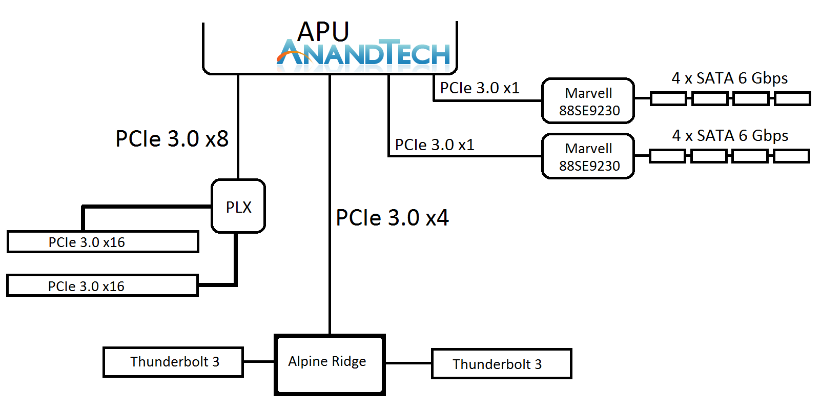
Ian plays a crazy game of PCIe Lego
The joy of PCIe and switches is that it becomes a mix and match game - there’s also the PCIe 3.0 x4 to the chipset. This can be used for non-chipset duties, such as anything that takes PCIe 3.0 x4 like a fast SSD, or potentially Thunderbolt 3. We discussed TB3 support, via Intel’s Alpine Ridge controller, and we were told that the AM4 platform is currently being validated for systems supporting AMD XConnect, which will require Thunderbolt support. AMD did state that they are not willing to speculate on TB3 use, and from my perspective this is because the external GPU feature is what AMD is counting on as being the primary draw for TB3 enabled systems (particularly for OEMs). I suspect the traditional motherboard manufacturers will offer wilder designs, and ASRock likes to throw some spaghetti at the wall, to see what sticks.


122 Comments
View All Comments
DanNeely - Friday, September 23, 2016 - link
X = 1Y = 2
Z = 3
HL3 confirmed for 2017 launch.
anatol1981 - Friday, September 23, 2016 - link
Please, correct L1D info - its wrong.anatol1981 - Friday, September 23, 2016 - link
As i can see, L1-I swapped with L1-D, please, reverse them^)Mr Perfect - Friday, September 23, 2016 - link
Any chance the enthusiast grade chipset will be fabbed at the more expensive 28nm or 16nm node? Highend systems could justify the cost.Tom Womack - Friday, September 23, 2016 - link
The cost of fabbing a device at a different node is conservatively fifty million dollars; you're talking about a total reimplementation and revalidation, followed by a complete new mask set. There aren't half a million people willing to pay $100 more for an indifferent AMD chipset fabricated on a slightly shinier process.Mr Perfect - Friday, September 23, 2016 - link
That's assuming that the highend chipset was designed for the 55nm process from the start and would need to be redesigned for 28nm. If they designed the highend stuff for 28nm right from the start, it would just be fabrication cost differences.You're probably right though. They probably didn't see a big enough benefit in doing the C380(or whatever it ends up being called) at a modern node.
patrickjp93 - Tuesday, September 27, 2016 - link
Intel must be able to do it for far less, because there's no way Coffee Lake will sell that well, and it's based on the Cannonlake architecture which was originally built with 10nm in mind.Kalelovil - Sunday, September 25, 2016 - link
The desktop enthusiast market is unlikely to care for the couple of watts of power that could save.For the laptop market where power matters a lot more, I expect the Zen APU to integrate more connectivity onto the die and do away with the south-bridge entirely.
patrickjp93 - Tuesday, September 27, 2016 - link
Those are cheaper nodes due to maturity, jsyk.starlightmica - Friday, September 23, 2016 - link
HP Canada's 510-p127c spec page:http://support.hp.com/ca-en/document/c05281246
AMD A12-9000
16GB DDR4
R7 450 2Gb GDDR5, 4K over DP1.2, HDMI 1.4
180W uATX PSU :(