Micron 3D NAND Update: 2D and 3D NAND Bit Crossover, Gen 2 Hits Production
by Anton Shilov on December 13, 2016 2:00 PM ESTMicron last week made two announcements regarding its transition to 3D NAND memory. According to the company, the output of 3D NAND at its fabs has surpassed the output of 2D NAND in terms of bits. Meanwhile, the costs of the first-generation 3D NAND are in line with expectations and the company is gearing up to start high-volume production of its second-gen 3D NAND in the coming weeks.
Crossover Reached
Ernie Maddock, CFO of Micron, said at the Barclays Technology Conference that the company had achieved a bit crossover between 2D and 3D NAND flash memory output. This means that total capacity of 3D NAND memory produced by Micron now exceeds the total capacity of 2D NAND memory made by the company. The bit crossover was a relatively easy target to hit because Micron’s 2D MLC and TLC NAND devices made using 16 nm process technology can store up to 128 Gb of data, whereas the capacity of the company’s 3D NAND IC is 256 Gb in MLC configuration and 384 Gb in TLC configuration. That said, once 3D wafer production started and yields hit certain levels, the balance between 2D NAND and 3D NAND output adjusts, and the bit crossover happens despite more 2D chips being producted.
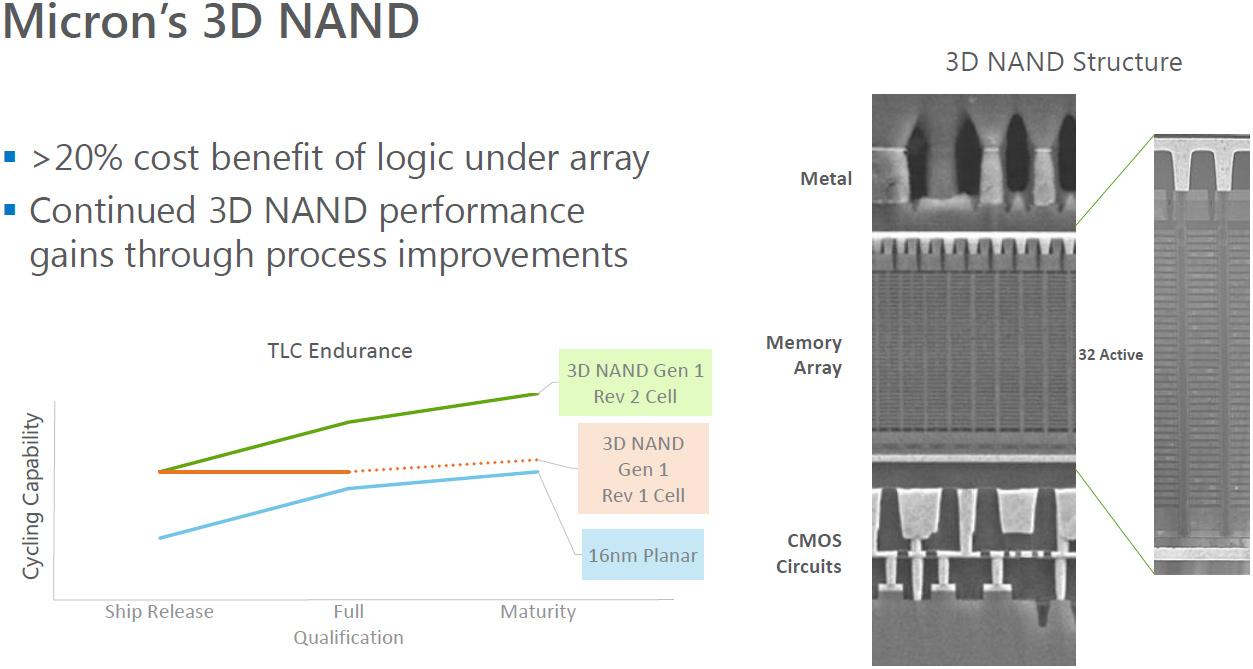
While balancing 2D and 3D NAND output seems easy on paper, it is not. Manufacturing technologies involved in the production of 2D and 3D NAND are completely different. 2D NAND relies on lithography, and in order to transit to a new fabrication process one needs to switch to more advanced step-and-scan systems. 3D NAND relies on deposition and etching: first, you need to deposit many layers (38 in case of Micron’s Gen 1 3D NAND) of thin films on top of a wafer in a uniform manner (alternating stack deposition) to build up word-lines, and then you need to etch millions of holes through them (high aspect ratio etch) to pave the way for bit lines. Everything is much more complex, even at a high level, but in general, the alternating stack deposition requires chemical vapor deposition (CVD) machines whereas high aspect ratio etch requires other tools. Lithography tools are not going anywhere, but the addition of extra CVD, high aspect ratio etch tools and other equipment vital to make 3D NAND to the fabs doubles or even quadruples the amount of space required to process the same amount of 2D NAND wafers (see details why at Semiconductor Engineering).
All things considered, it is not easy at all to start making 3D NAND in a fab that is already making 2D NAND. Flash memory manufacturers have to halt production of existing memory, add the equipment (which may involve removal of certain existing tools because space is precious), tune everything, and start production. Keeping in mind that Micron started high-volume manufacturing of 3D NAND sometime in early 2016, so hitting a bit output crossover in less than a year looks rather impressive given complexities with the conversion of capacities, yet predictable, given capacity improvements that the 3D NAND ICs have over planar ones.

Now, as Micron is transiting its leading-edge NAND flash manufacturing capacity to 3D, it is also implementing its new strategy of focusing on actual products rather than on commodity chips. This means that as the company is winding down its 2D NAND production and ramping up 3D NAND, it also reduces sales of all kind of NAND chips to third parties. For example, independent SSD manufacturers who used to buy Micron’s 2D NAND for their products will gradually have to turn to others like Toshiba for 2D NAND. Moreover, Micron seems to supply 3D NAND to only one third party vendor now, ADATA, an indicator that the company is gradually leaving the spot/contract market of NAND flash chips. Note that this does not mean that Micron will never sell NAND to any third party at all, because a commercial company is supposed to make money. Keeping in mind that Toshiba/SanDisk as well as SK Hynix also do not supply SSD-grade 3D NAND to third parties, ADATA remains the only independent maker of actual drives that ships products featuring 3D NAND memory.
Gen1 3D NAND: Costs Are In Line
During the presentation at the conference, the CFO of Micron also indicated that the cost-per-bit of the company’s 3D NAND flash is consistent with its original projections and is 20% – 25% lower compared to 16 nm 2D NAND on the cost-per-bit basis.
When it comes to costs, the situation is also complicated. Process technologies for 2D NAND and 3D NAND manufacturing are completely different and even though Micron’s (IMFT’s) 128 Gb 2D NAND and 384 Gb 3D NAND have similar die sizes (at 173 mm2 and 168.5 mm2 they are close, but not the same), the actual per-chip costs of these two chips is not the same even at the same yield. Meanwhile, yields of chips produced using different fabrication processes are different and that naturally affects costs. Moreover, keep in mind that manufacturers are only learning how to produce 3D NAND and it is unlikely that the yields are high. Then again the massive increases of per-chip capacities can offset chip yield issues to a certain degree. After all, if Micron’s per-bit costs are lower with 3D NAND and the company sells such memory at a profit, this is all that matters to the firm and its investors.
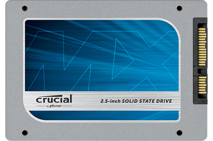
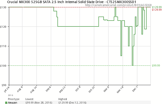
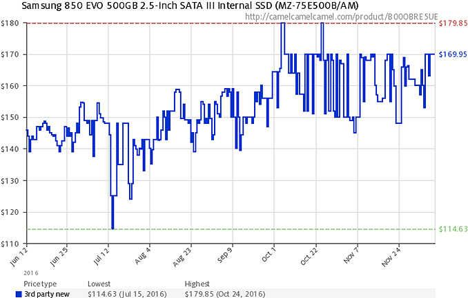
What matters for the end users are the end-products: affordable SSDs and other products based on NAND flash memory. We are hearing that in the recent months Micron has been pushing its Crucial MX300-series SSDs into the channel aggressively, which is an indicator that the volumes of the drives it can produce are fairly high. Moreover, if the company is trying to compete using relatively affordable prices (well, a quick check of pricing trends at Amazon shows that Micron’s MX300 525 GB did not get more expensive over the past couple of months, unlike Samsung’s 850 EVO 500 GB, and is more affordable than the rival in general), this may point out that its costs are more or less comfortable and Micron feels that it can increase unit sales of its SSDs.
It is about time for Micron to be aggressive with its SSDs. Over the past few quarters, Micron’s unit share of the SSD market dropped from 7.1% in Q1 2015 to 3.9% in Q2 2016 (data by TrendFocus), while its unit shipments decreased from 1.65 million units to 1.25 million units in the same timeframe. Apparently, Micron is plotting a comeback using its 3D NAND-based SSDs. A good news for the company is that the latest MX300 lineup featuring Gen 1 3D TLC NAND lacks cheap 120/128 GB configurations meaning that Micron does not have to participate in the race to the bottom and thus might enjoy higher ASPs.
Gen 2 3D TLC NAND Incoming
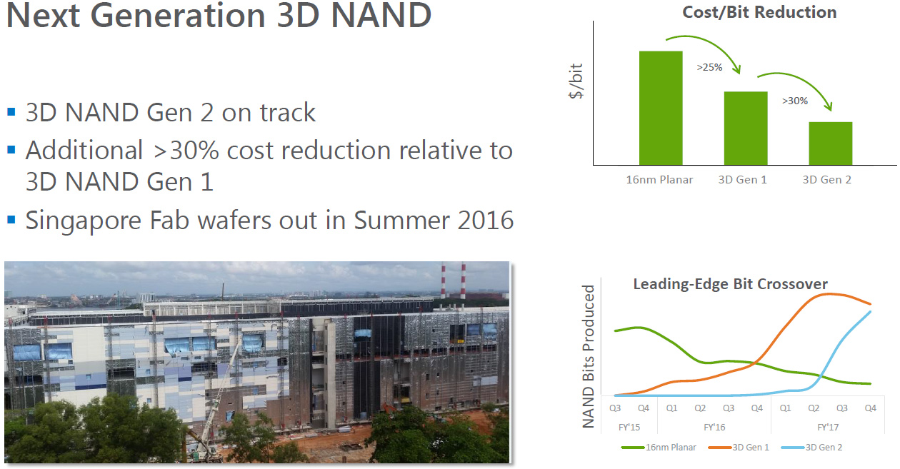
During his presentation at the Barclays Technology Conference, the high-ranking executive from Micron also disclosed the company’s updated plans regarding its second-generation 3D NAND and the Fab 10X in Singapore.
“We have a couple of exciting things on the horizon, […] Gen 2, which is a 64-layer product, that will be in the manufacturing facility as we exit this year,” said Mr. Maddock.
First and foremost, Micron said that its second-generation 3D NAND is about to hit mass production, which is in line with the company’s expectations to start HVM of Gen 2 3D NAND in early FY2017 (which began in September ‘16). Secondly, as the company said before, its second-gen 3D NAND would be produced at its Fab 10X in Singapore, hence the ramp up of Gen 2 3D NAND means the new fab is coming online. Thirdly, Micron confirmed that the company’s Gen 2 3D NAND features 64 active layers (which represents word lines in 3D NAND architecture.
It is unknown how many layers in total will Micron’s Gen 2 3D NAND chips have, but it is important to note that various experts indicate that once the number of layers within a 3D NAND IC reaches ~60 or ~70, new challenges arise.
According to Er-Xuan Ping, managing director of memory and materials within the Silicon Systems Group at Applied Materials, current etching tools cannot “drill holes” in a structure that contains ~60 or ~70 layers. To tackle that issue, Micron and other makers of NAND are reportedly developing a technique called string stacking. From a high-level point of view, string stacking involves stacking individual 3D NAND devices on top of each other in a way that interconnects the NAND strings and allows the NAND controller to see the whole IC as a single component with a unified address space and manage it this way. Linking of two NAND strings is an extremely tricky process because everything has to be perfectly aligned and that is a hard thing to do. A good thing is that string stacking enables to build 3D NAND ICs with hundreds of layers, potentially meaning extreme densities (and complexities) going forward.
“This is the limitation,” said Er-Xuan Ping, managing director of memory and materials within the Silicon Systems Group at Applied Materials. “Up to a certain point, a single-string is limited by etching or other process steps.”

Micron is not the only company to announce and produce a 64-layer 3D NAND component. Samsung and Toshiba/Western Digital are also ready with their 64-layer 3D flash memory devices. More interestingly, none of the three companies have mentioned string stacking in their initial press releases covering the topic (a rumor has it that Micron has demonstrated a 64-layer 3D NAND chip with string stacking to some of its partners). Perhaps, they have found a way etch deep holes using the current equipment, or just decided not to mention peculiarities in their formal announcements.
Samsung announced its fourth-generation 64-layer V-NAND ICs in August and said that it would start mass production of actual products based on the devices in Q4 2016. Initially, Samsung’s fourth-gen 64-layer V-NAND ICs will be available in 512 Gb TLC configurations (an MLC configuration is also possible, but with a lower capacity) and will support interface speed of 800 Mbps to reduce the performance penalty that comes from consolidating more flash onto fewer independent chips. After Samsung tests its 64-layer V-NAND flash in removable storage and mobile devices, it will start using it for SSDs sometimes in 2017.
Toshiba/Western Digital have been sampling their third-generation 64-layer BiCS NAND memory with OEMs for a while now and Western Digital even promised to start shipping removable storage devices based on such memory in Q4 2016. Initially, BICS3 chips will be offered in TLC configurations with 256 Gb capacity, but eventually their capacity will increase to 512 Gb. It is noteworthy that Western Digital considers the 64-layer BiCS 3D NAND as SSD-grade memory, which means we are finally going to see SSDs featuring 3D NAND from Toshiba and WD in 2017.
Unlike its competitors, Micron yet has to make a formal announcement concerning its upcoming 3D NAND devices, but the company has already released some of the details about the chips on different occasions. Early this year Micron described its 3D TLC NAND chip with 768 Gb capacity at the IEEE International Solid-State Circuits Conference. The company then disclosed at the NASDAQ 34th Investor Program Conference in June that its Gen 2 3D NAND would “double the density” of its first-generation product (i.e., 384 Gb => 768 Gb) and would reduce per-bit costs by up to 30%. This month, Micron confirmed that its second-generation 3D NAND is set to have 64 layers.
Apparently, it looks like Micron’s Gen 2 3D NAND chips will indeed have 768 Gb capacity (96 GB) and 64 layers (probably 512 Gb MLC chips are also possible, but we cannot confirm that). Meanwhile, the massive increase of density has pros and cons: on the one hand, you can build high-capacity storage devices in miniature form-factors (how about a 3 TB single-sided M.2?), and one the other hand you cannot build entry-level devices with decent performance due to lack of parallelism. With its Gen 1 3D TLC NAND Micron already had to solve this dilemma this year, which is why it had to abandon 120/128 GB SSD configuration. Next year it will have to make a similar decision in regards of 256 GB drives. Other points of concern about 768 Gb 3D TLC NAND chips are their real-life yields and costs, but that is something we are going to learn about only several quarters down the road.


14 Comments
View All Comments
jamyryals - Wednesday, December 14, 2016 - link
Terrific article!doggface - Wednesday, December 14, 2016 - link
Great article. Thanks for the insight.I would think if they are able to get higher densities, such as 512Gb we might see some reductions in price again. A 30% reduction in price would be appreciated.
Ultimately if 500GB drives get to the point where it is viable in a $1000 laptop, that would be good enough.
sonicmerlin - Wednesday, December 14, 2016 - link
I think what they're saying is that 512 GB will become the minimum size in those laptops, otherwise you'll sacrifice a lot of speed (*cough* iPhone 7 *cough*).dealcorn - Wednesday, December 14, 2016 - link
I bought a Crucial MX300 750GB SATA 2.5" Drive (CT750MX300SSD1) on Thanksgiving day from Amazon,com LLC for $99.99. The price of 13.33 cents per gigabyte seemed like a reasonable sale price.