The AMD Zen and Ryzen 7 Review: A Deep Dive on 1800X, 1700X and 1700
by Ian Cutress on March 2, 2017 9:00 AM ESTThe High-Level Zen Overview
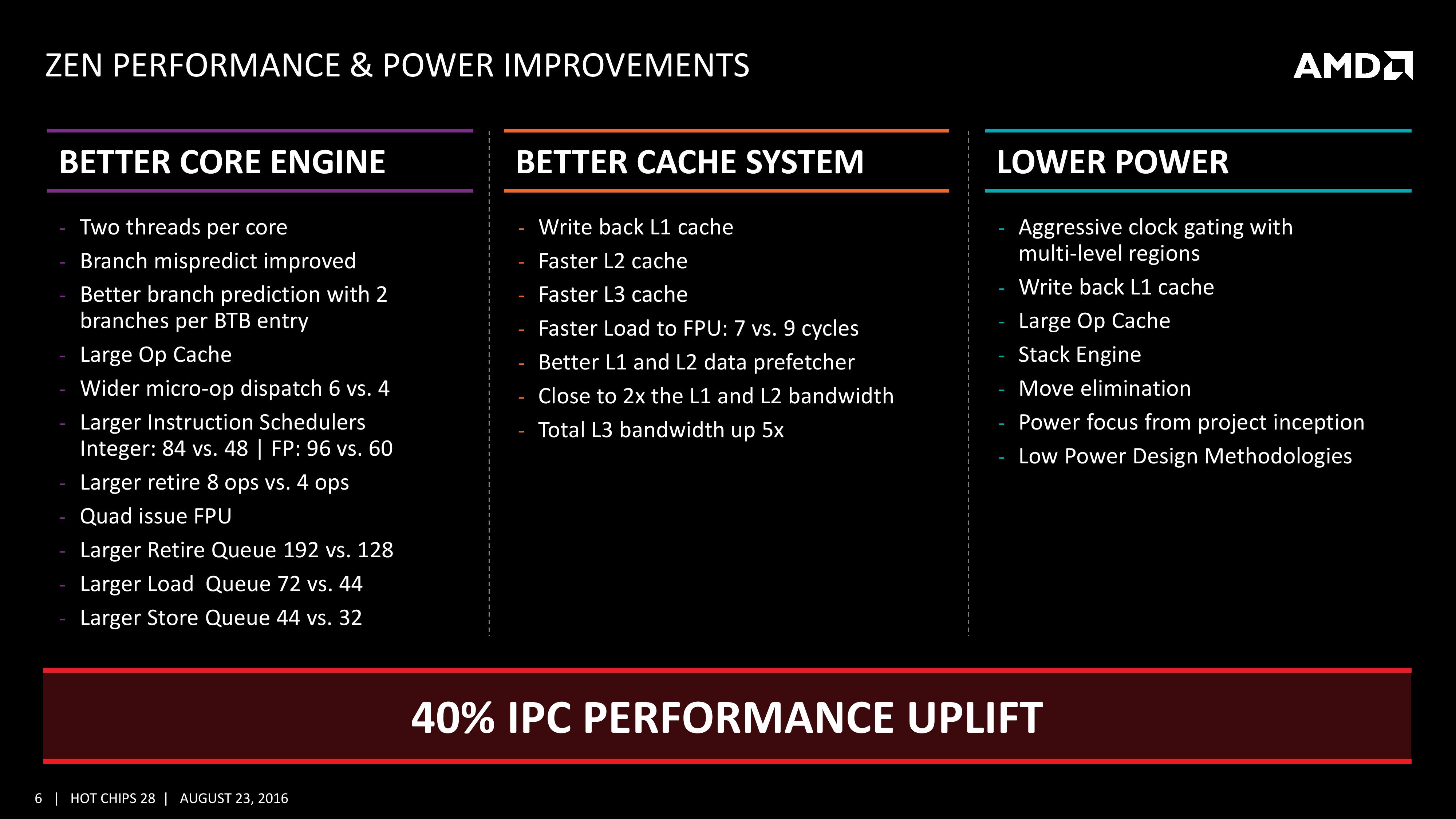
AMD is keen to stress that the Zen project had three main goals: core, cache and power. The power aspect of the design is one that was very aggressive – not in the sense of aiming for a mobile-first design, but efficiency at the higher performance levels was key in order to be competitive again. It is worth noting that AMD did not mention ‘die size’ in any of the three main goals, which is usually a requirement as well. Arguably you can make a massive core design to run at high performance and low latency, but it comes at the expense of die size which makes the cost of such a design from a product standpoint less economical (if AMD had to rely on 500mm2 die designs in consumer at 14nm, they would be priced way too high). Nevertheless, power was the main concern rather than pure performance or function, which have been typical AMD targets in the past. The shifting of the goal posts was part of the process to creating Zen.
This slide contains a number of features we will hit on later in this piece, but covers a number of main topics which come under those main three goals of core, cache and power.
For the core, having bigger and wider everything was to be expected, however maintaining a low latency can be difficult. Features such as the micro-op cache help most instruction streams improve in performance and bypass parts of potentially long-cycle repetitive operations, but also the larger dispatch, larger retire, larger schedulers and better branch prediction means that higher throughput can be maintained longer and in the fastest order possible. Add in dual threads and the applicability of keeping the functional units occupied with full queues also improves multi-threaded performance.
For the caches, having a faster prefetch and better algorithms ensures the data is ready when each of the caches when a thread needs it. Aiming for faster caches was AMD’s target, and while they are not disclosing latencies or bandwidth at this time, we are being told that L1/L2 bandwidth is doubled with L3 up to 5x.
For the power, AMD has taken what it learned with Carrizo and moved it forward. This involves more aggressive monitoring of critical paths around the core, and better control of the frequency and power in various regions of the silicon. Zen will have more clock regions (it seems various parts of the back-end and front-end can be gated as needed) with features that help improve power efficiency, such as the micro-op cache, the Stack Engine (dedicated low power address manipulation unit) and Move elimination (low-power method for register adjustment - pointers to registers are adjusted rather than going through the high-power scheduler).
The Big Core Diagram
We saw this diagram last year, showing some of the bigger features AMD wants to promote:
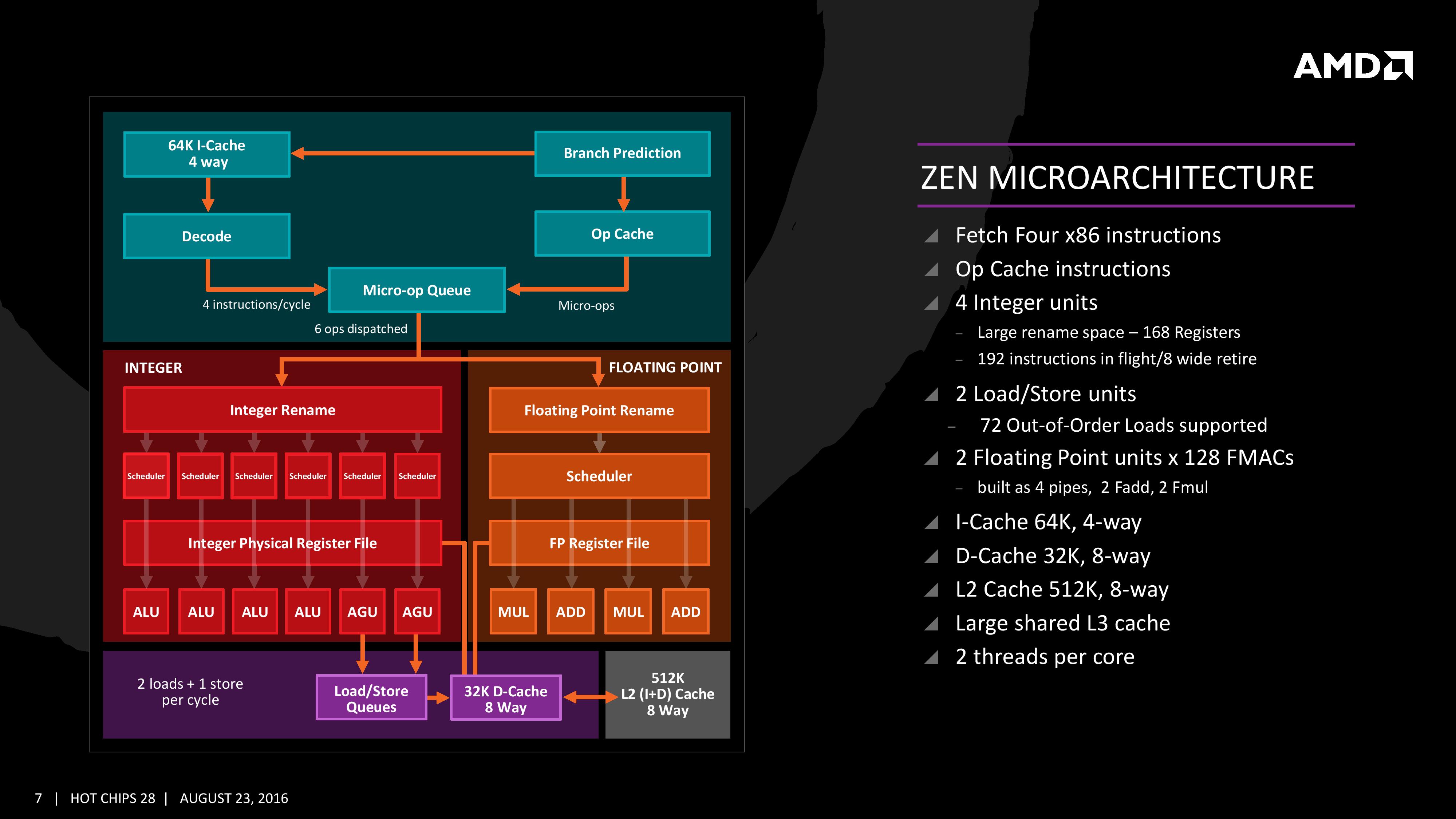
The improved branch predictor allows for 2 branches per Branch Target Buffer (BTB), but in the event of tagged instructions will filter through the micro-op cache. On the other side, the decoder can dispatch 4 instructions per cycle however some of those instructions can be fused into the micro-op queue. Fused instructions still come out of the queue as two micro-ops, but take up less buffer space as a result.
As mentioned earlier, the INT and FP pipes and schedulers are separated, however the INT rename space is 168 registers wide, which feeds into 6x14 scheduling queues. The FP employs as 160 entry register file, and both the FP and INT sections feed into a 192-entry retire queue. The retire queue can operate at 8 instructions per cycle, moving up from 4/cycle in previous AMD microarchitectures.
The load/store units are improved, supporting a 72 out-of-order loads, similar to Skylake. We’ll discuss this a bit later. On the FP side there are four pipes (compared to three in previous designs) which support combined 128-bit FMAC instructions. These can be combined for one 256-bit AVX, but beyond that it has to be scheduled over multiple instructions.


574 Comments
View All Comments
Notmyusualid - Saturday, March 4, 2017 - link
Then why was the first 7700K at 199th place?The results dont' tie in with your retort.
Notmyusualid - Saturday, March 4, 2017 - link
And futhermore, 3dmark11 is a respected benchmark, that I and other PC games I know, use regularly.If you visit the 3DMark website, you will see LOADS of 3dmark11 results 'ticking in' on the global map.
And personally, every PC I've played with high 3dmark11 numbers has played games better than ones that have lower numbers, so you can't discount it. It works, whether you like it or not.
7700K, 199th place for 1080. Look it up. All above are X79, X99 type boards.
Aerodrifting - Sunday, March 5, 2017 - link
That just proved you really don't know anything about gaming, No point wasting my timNotmyusualid - Monday, March 6, 2017 - link
Then don't.Blissfull in ignorance..
Notmyusualid - Monday, March 6, 2017 - link
@ AerodriftingIn addition to MY comments on 3dMark11, try this from Guru3d, unless of course YOU always know better:
Quote:
3DMark 11 is the latest version of what is probably the most popular graphics card benchmark series. Designed to measure your PC's gaming performance, 3DMark 11 makes extensive use of all the new features in DirectX 11 including tessellation, compute shaders and multi-threading. Trusted by gamers worldwide to give accurate and unbiased results, 3DMark 11 is the best way to consistently and reliably test DirectX 11 under game-like loads. We test 3DMark 11 in performance mode which will give is a good indication of graphics card performance in the low, mid-range and high end graphics card segment.
And Link:
https://www.guru3d.com/articles_pages/geforce_gtx_...
And with that, I'm done here.
divertedpanda - Saturday, March 4, 2017 - link
"Everyone Know" ....... Except... Numbers don't lie.tmach - Thursday, March 2, 2017 - link
Yes and no. The $340 7700k beats the $1,000 6900k in gaming at stock speeds, too. That just goes to show that 8-cores still aren't for gaming, no matter how much some people (AMD included) want to make it a thing.GatesDA - Thursday, March 2, 2017 - link
They're not aimed at gamers; they're undercutting Intel's 6- and 8-core chips. Multithreading's the only reason to get a Ryzen 7, since the 6-core Ryzen 5 1600X will have the same clock speeds as the Ryzen 7 1800X for way less. Their unrevealed 4-core chips will probably be the gaming sweet spot.nader_21007 - Thursday, March 2, 2017 - link
well yeah you could stick more PCIe3 lanes and quad memory channels up your @$$.what use have these if the performance of your $1000 CPU is inferior to a $500 CPU? tell me.
prisonerX - Thursday, March 2, 2017 - link
Wow, gamers, that self-important 5% of the market. They'll never leave Intel anyway. When your customers are such rubes they'll pay top dollar for chips that contain 65% useless functionality, you can abuse them as much as you like. Gamers will still be buying 2% performance gains for generations to come.