AMD Unveils the Radeon Vega Frontier Edition: Vega Starts in the Pros
by Ryan Smith on May 17, 2017 2:45 AM EST- Posted in
- GPUs
- AMD
- Radeon
- Machine Learning
- Vega
- Radeon Pro
- Vega Frontier Edition

It feels like the build-up to Vega has been just shy of forever. And in a way it has been: AMD first announced the architecture back in March of 2016, and we’ve known for almost as long that Polaris would be a volume play, not a play for the high performance market. It would be Vega that would be AMD’s next high-end GPU, and true successor to 2015’s unique (if mistimed) Fiji GPU.
Since then AMD has slowly been releasing details on the Vega architecture. Bits and pieces related to the Playstation 4 Pro, which incorporated some Vega features, and then a much more significant information dump at the start of this year with their Vega teaser, closely aligned with their associated announcement of the Radeon Instinct accelerator, which set some pretty specific guidelines for what kind of performance AMD was aiming for. Until today all we’ve known for sure is that Vega would be ambitious, but not unrealistic, and that AMD wanted to launch it by the end of June.
So for today’s AMD Financial Analyst Day, AMD has released a little bit more information as part of the next step of their campaign. The first Vega product to be released has a name, it has a design, and it has performance figures. Critically, it even has a release date. I hesitate to call this a full announcement in the typical sense – AMD is still holding some information back until closer to the launch – but we now finally have a clear picture of where the Vega generation kicks off for AMD.
Say hello to the Radeon Vega Frontier Edition.
| AMD Workstation Card Specification Comparison | ||||||
| Radeon Vega Frontier Edition | Radeon Pro Duo (Polaris) | Radeon Pro WX 7100 | Radeon Fury X | |||
| Stream Processors | 4096 | 2 x 2304 | 2304 | 4096 | ||
| Texture Units | ? | 2 x 144 | 144 | 256 | ||
| ROPs | 64? | 2 x 32 | 32 | 64 | ||
| Boost Clock | ~1.59GHz | 1243MHz | 1243MHz | 1050MHz | ||
| Single Precision | ~13 TFLOPS | 11.5 TFLOPS | 5.7 TFLOPS | 8.6 TFLOPS | ||
| Half Precision | ~26 TFLOPS | 11.5 TFLOPS | 5.7 TFLOPS | 8.6 TFLOPS | ||
| Memory Clock | ~1.88Gbps HBM2 | 7Gbps GDDR5 | 7Gbps GDDR5 | 1Gbps HBM | ||
| Memory Bus Width | 2048-bit | 2 x 256-bit | 256-bit | 4096-bit | ||
| Memory Bandwidth | ~480GB/sec | 2x 224GB/sec | 224GB/sec | 512GB/sec | ||
| VRAM | 16GB | 2 x 16GB | 8GB | 4GB | ||
| Typical Board Power | ? | 250W | 130W | 275W | ||
| GPU | Vega (1) | Polaris 10 | Polaris 10 | Fiji | ||
| Architecture | Vega | Polaris | Polaris | GCN 1.2 | ||
| Manufacturing Process | GloFo 14nm | GloFo 14nm | GloFo 14nm | TSMC 28nm | ||
| Launch Date | 06/2017 | 05/2017 | 10/2016 | 06/24/15 | ||
| Launch Price | (A profitable number) | $999 | $649 | $649 | ||
How AMD is going to sell this card and its target market is a huge subject (and arguably the most important aspect of today’s announcement) but I think everyone would rather dive into the specs first. So let’s start there.
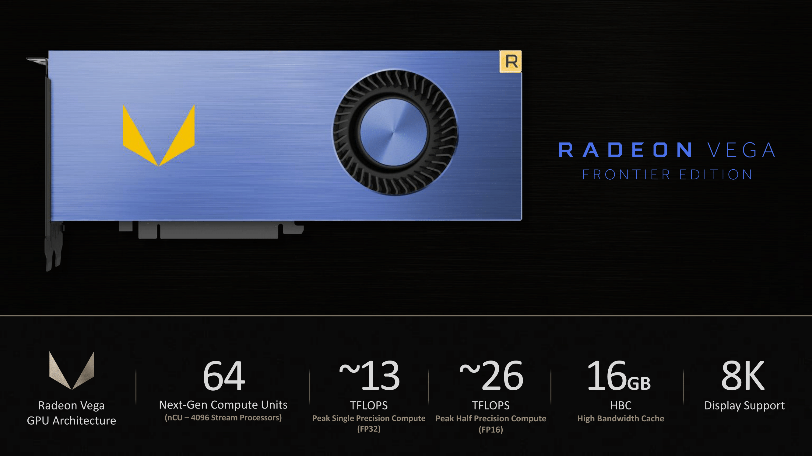
The Radeon Vega Frontier Edition is meant to be a powerhouse of a card for AMD. While we’re still not quite sure which Vega chip we’re looking at – AMD has confirmed two chips so far, and it now looks like the second chip is going to be farther down the line – the Vega that we are getting now is AMD’s high-end play. And this is reflected in the Vega Frontier Edition high performance specifications.
AMD previously indicated with the Radeon Instinct MI25 announcement that they would be targeting 25 TFLOPS or better of half precision (FP16) performance on their high-end Vega parts, and the Vega Frontier Edition will be delivering on the “or better” part of that, with performance in the ballpark of 26 TFLOPS. With the caveat that AMD isn’t providing precise numbers at this time – like the Polaris launch, they’re being a bit unspecific – this indicates that AMD is hitting their earlier performance goals.
Furthermore, as part of today’s announcement we finally know that the Vega Frontier Edition will ship with 64 CUs (4096 stream processors), which also allows us to narrow down the clockspeeds of the card. To hit 26 TFLOPS FP16, the card needs to be able to boost to around 1.59GHz. This is particularly notable because AMD’s reference Polaris designs only go to 1.34GHz, which means that AMD is expecting to clock Vega cards a good bit higher than their Polaris cards.
Hitting these high clockspeeds is important for AMD, because while Vega is slated to be a powerful chip, in terms of execution width it’s actually not an especially wide chip. With 64 CUs, the Vega FE is no wider than AMD’s last-generation Fiji-based cards like the Radeon Fury X, which had the same 64 CU configuration. This means that relative to its predecessor, Vega FE is going to rely on the combination of significantly higher clockspeeds and its architectural enhancements to deliver the big performance gains AMD is touting for the card.

Meanwhile, although we now have a good picture of the CU situation for Vega FE, we have a bit of a mystery on our hands with the ROP situation. AMD has not disclosed the number of ROPs, but it has disclosed that the card will have a pixel fillrate of about 90 Gigapixels/second, which doesn’t divide neatly into the earlier clockspeed. It’s quite likely that we’re looking at a 64 ROP design and that AMD’s figures are factoring in a more conservative clockspeed (e.g. the base clock rather than the boost clock). But for the moment, this dichotomy means that the ROP configuration of the Vega FE isn’t as clear as the CU configuration.
Moving on, AMD has confirmed that the Vega FE will have approximately 480GB/sec of memory bandwidth, and in a big surprise, that this will come from 16GB of HBM2 memory. AMD has been heavily promoting their use of HBM2 and what it means for their memory architecture – the High Bandwidth Cache Controller – particularly banking on the fact that the HBM2 specification allows for memory speeds of up to 2Gbps/pin. Coupled with the fact that we’ve already seen an early Vega chip with 2 HBM2 stacks (indicating a 2048-bit bus), and AMD’s figures confirm that they’re going to be coming very close to 2Gbps for the Vega FE. The card’s 480GB/sec of bandwidth means that the HBM2 stacks need to be clocked at 1.875GHz, just short of that 2Gbps figure.
However the far more interesting news here isn’t the bandwidth, but the amount of total HBM2 memory. AMD has revealed that the Vega FE will ship with 16GB of memory, a figure that until today didn’t look to be possible. And to be honest, we’re still not sure how AMD is doing it.
Along with the higher data rate of HBM2, the other major feature of the newer HBM specification is that it allows for much higher capacity stacks, up to 4GB for a 4 layer (4-Hi) stack, or 8GB for an 8 layer (8-Hi) stack, solving the capacity issues that dogged the HBM1-powered Fiji GPU. However to date, neither Samsung nor SK Hynix have offered 8-Hi HBM2 in their parts catalogs. No specific reason has been given, but the use of TSVs means that the greater the number of layers, the harder the memory is to assemble. For the moment, a pair of 8-Hi stacks is by far the most likely explanation for how AMD has put 16GB of VRAM on the Vega FE. However until we hear more from AMD, it’s not the only possibility, and given that 8-Hi HBM2 still isn’t on anyone’s parts list, it may be that AMD has adopted more creative measures to get this much VRAM on a Vega card.
Rounding out the specifications, as AMD’s focus in today’s announcement was on compute performance and memory, the company hasn’t disclosed too much else about the hardware itself. The TDP has not been announced, however as we’re looking at a high-end card, 250W or better is a very good assumption, especially as AMD’s renderings of the Vega FE cards all show the card sporting a pair of 8-pin PCIe power sockets.

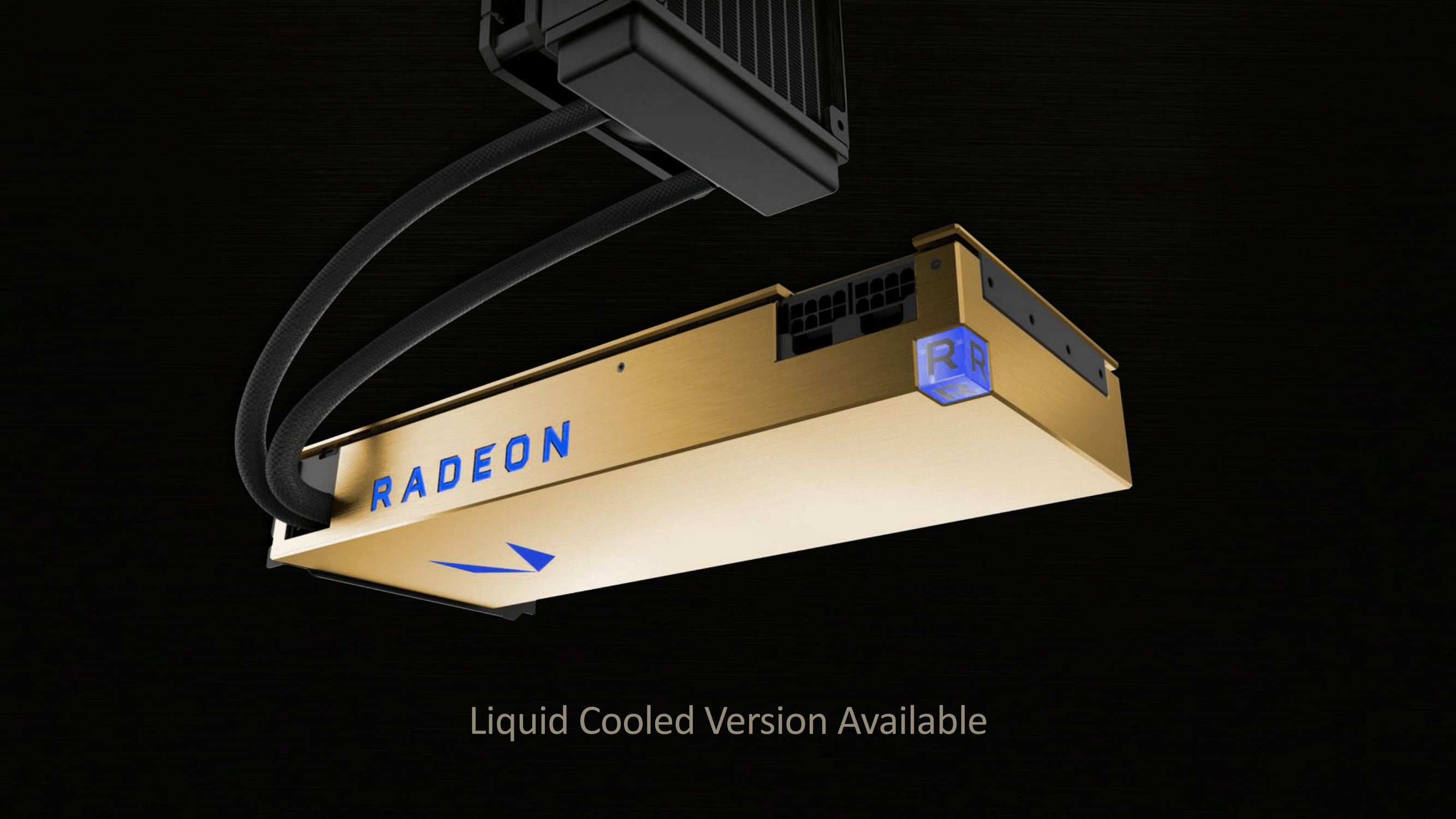
What we do know is that there will be two different Vega FE cards, which AMD is calling the Vega Frontier Blue Edition and the Vega Frontier Gold Edition. Information on the differences between these cards is very limited, but from the information AMD has provided, the Blue Edition will be a traditional blower-cooled card, while the Gold Edition will be taking a page from the Radeon Fury X and will feature an external radiator attached via an integrated closed loop liquid cooling system (CLLC). The use of a CLLC on the Fury X in 2015 made it a very quiet card, but at the same time it was also a necessary move due to its 275W TDP. So this may be a sign that the Gold card will have a particularly high TDP.
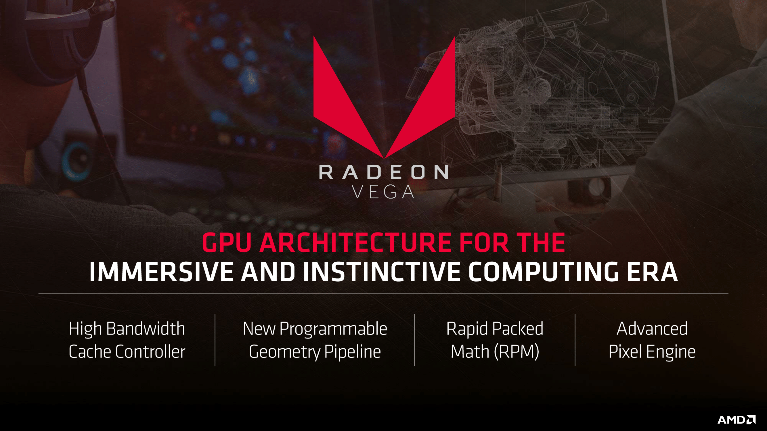
Otherwise at an architectural level, AMD hasn’t revealed any further details on the Vega architecture, and indeed it’s not clear if there’s much they left uncovered in this winter’s Vega architecture teaser. HBM2, the improved geometry engine, the new FP16-capable CUs, and the tiling rasterizer were all touched upon in today’s announcement. And as mentioned previously, these new architectural optimizations, along with Vega FE’s high clockspeed, are going to be the major components of the card’s performance.
Finally, with today’s announcement AMD has further narrowed down the launch date of their first Vega cards. The Vega Frontier Edition will be the first cards to ship, and as per the company’s earlier promise of an H1’17 launch, the cards will be available in late June. AMD has not announced a price for the cards yet, and like the detailed specifications themselves, I expect we’ll see that closer to next month’s launch.
But what is clear right now is that the Vega Frontier Edition is not meant to be a consumer gaming card, and that takes us into what I think is the more interesting aspect of today’s announcement: the target market.


134 Comments
View All Comments
vladx - Wednesday, May 17, 2017 - link
Indeed, RX 480 with 5.8 TFLOPs is about equal to 1060 GT with 3.9 TFLOPs so we need to see how much improved Vega really is.juliovillaz1990 - Wednesday, May 17, 2017 - link
You are wrong.. the 1060 its 5 tflops aproximately. You're nota taking un consideration the auto oc feature of Pascal cards, the 1060 auto overclocks nearly 2000mhz si its not 3.9 tflopsYojimbo - Thursday, May 18, 2017 - link
Where do you get this from? In what games is the GTX 1060 averaging 2000 MHz without overclocking?Regardless, it doesn't matter. You are agreeing that AMD's listed TFLOPs are worth less than NVIDIA's listed TFLOPs, which was the point of the thread. Whether it's true because NVIDIA's cards are able to consistently clock above their listed frequencies or because NVIDIA's architecture spends less time waiting around doesn't matter. (As long as NVIDIA's cards stay within their thermal envelopes, which they seem to do better than AMD's, in fact.)
Alexvrb - Sunday, May 21, 2017 - link
Gaming performance isn't the best measure when talking about professional graphics cards. It's silly to say "X TFLOPS on card A equals Y TFLOPS on card B because of gaming benchmarks" when discussing professional cards that are used for different software.vladx - Monday, May 22, 2017 - link
Don't know who you're responding to, I compared RX 480 and 1060 GT which neither being part of pro segment and I specifically mentioned we need a better picture of Vega's architecture.Yojimbo - Monday, May 22, 2017 - link
"Gaming performance isn't the best measure when talking about professional graphics cards. It's silly to say "X TFLOPS on card A equals Y TFLOPS on card B because of gaming benchmarks" when discussing professional cards that are used for different software."I think vladx's use of gaming performance to demonstrate that TFLOPs cannot be used to directly compare performance between two different architectures is perfectly fine. The person he replied to performed just such a comparison. And although vladx did say that Vega has to improve for AMD to catch up to NVIDIA, and perhaps that's not true in professional applications (I don't really know), the original post should not be assumed to be about professional performance. The OP simply said "I really want Vega to succeed", not "I really want this Vega Frontier Edition to succeed". I'm guessing he meant Vega in all its incarnations.
extide - Thursday, May 18, 2017 - link
When it comes to actual FLOPs ... FLOPS are FLOPS, they are the same. When it comes to how FLOPS translate to gaming performance .. that's another discussion, yes.CiccioB - Thursday, May 18, 2017 - link
No, and no.A TFLOPS means nothing at all. Because and operation is not like another.
We are used to FMA OPS to calculate theoretical peak TFLOPS capacities, but those do not really mean nothing. How many FMA do you use in an algorithm? How long can you sustain many FMA one after the other before bandwidth do fed them becomes a bottleneck?
A TFLOPS is not a precise unit of measure. It's just a "standard" way to classify computing devices. It may be that my device can't do FMA in a single cycle, so having half of your teorethica computational peak, but I may go faster than you.
So again a TFLOPS means nothing. What it really counts is the efficiency at which the architecture execute complex algorithms (and that is before you tale into account other resources like ROPS or TMUs or geometric management for a 3D pipeline).
By what we have seen today, nvidia is way more efficient than AMD in both area/perfomance and w/performance.
fanofanand - Wednesday, May 24, 2017 - link
Nvidia is using a bigger die to get similar numbers. Not sure where the area/performance you speak of stems from. AMD appears to be cheaper in a $/performance and area/performance comparison with Nvidia's latest and greatest design. I'm sure someone will correct me if I'm wrong, but the new Nvidia die is at the TSMC reticle limit.frenchy_2001 - Wednesday, May 24, 2017 - link
If you're talking about Volta, you're right, it is a much bigger die. What it is NOT though, is a competitor for this card. This Vega boasts 13TFlops, Volta boasts 120TFlops per chip for DNN (FP16 matrix multiply/add). It will also sell for a much higher price (Volta mezzanine cards are around $16k each). This is like comparing a Formula1 car and a Lexus. Not the same usage or market.This is supposed to compete with Titan XP. In that comparison, AMD uses much more expensive RAM (HBM2 vs GDDR5X) and die size is so far undisclosed, but past chips size and power consumption have not been in AMD's favor.