NVIDIA Reveals Next-Gen Turing GPU Architecture: NVIDIA Doubles-Down on Ray Tracing, GDDR6, & More
by Ryan Smith on August 13, 2018 8:20 PM EST- Posted in
- GPUs
- Raytrace
- CUDA
- Quadro
- NVIDIA
- Restructuring
- GDDR6
- Tensor
- Quadro RTX
- Turing
Moments ago at NVIDIA’s SIGGRAPH 2018 keynote presentation, company CEO Jensen Huang formally unveiled the company’s much awaited (and much rumored) Turing GPU architecture. The next generation of NVIDIA’s GPU designs, Turing will be incorporating a number of new features and is rolling out this year. While the focus of today’s announcements is on the professional visualization (ProViz) side of matters, we expect to see this used in other upcoming NVIDIA products as well. And by the same token, today’s reveal should not be considered an exhaustive listing of all of Turing’s features.
Hybrid Rendering & Neural Networking: RT & Tensor Cores
So what does Turing bring to the table? The marquee feature, at least for NVIDIA’s ProViz crowd, is on hybrid rendering, which combines ray tracing with traditional rasterization to exploit the strengths of both technologies. This announcement is essentially a continuation of NVIDIA’s RTX announcement from earlier this year, so if you thought that announcement was a little sparse, well then here is the rest of the story.
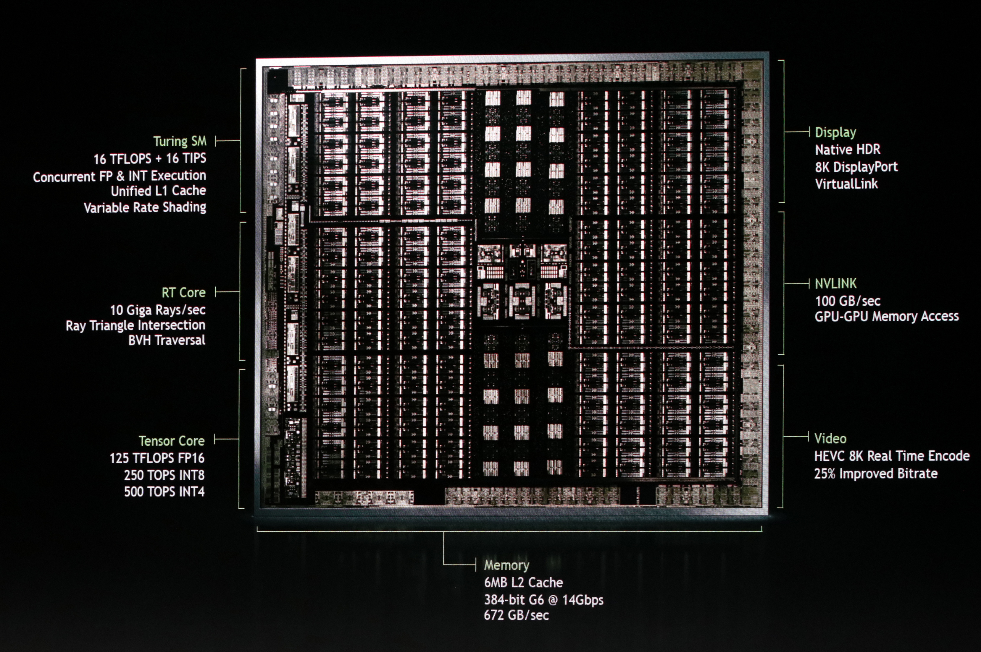
The big change here is that NVIDIA is going to be including even more ray tracing hardware with Turing in order to offer faster and more efficient hardware ray tracing acceleration. New to the Turing architecture is what NVIDIA is calling an RT core, the underpinnings of which we aren’t fully informed on at this time, but serve as dedicated ray tracing processors. These processor blocks accelerate both ray-triangle intersection checks and bounding volume hierarchy (BVH) manipulation, the latter being a very popular data structure for storing objects for ray tracing.
NVIDIA is stating that the fastest Turing parts can cast 10 Billion (Giga) rays per second, which compared to the unaccelerated Pascal is a 25x improvement in ray tracing performance.
The Turing architecture also carries over the tensor cores from Volta, and indeed these have even been enhanced over Volta. The tensor cores are an important aspect of multiple NVIDIA initiatives. Along with speeding up ray tracing itself, NVIDIA’s other tool in their bag of tricks is to reduce the amount of rays required in a scene by using AI denoising to clean up an image, which is something the tensor cores excel at. Of course that’s not the only feature tensor cores are for – NVIDIA’s entire AI/neural networking empire is all but built on them – so while not a primary focus for the SIGGRAPH crowd, this also confirms that NVIDIA’s most powerful neural networking hardware will be coming to a wider range of GPUs.
New to Turing is support for a wider range of precisions, and as such the potential for significant speedups in workloads that don't require high precisions. On top of Volta's FP16 precision mode, Turing's tensor cores also support INT8 and even INT4 precisions. These are 2x and 4x faster than FP16 respectively, and while NVIDIA's presentation doesn't dive too deep here, I would imagine they're doing something similar to the data packing they use for low-precision operations on the CUDA cores. And without going too deep ourselves here, while reducing the precision of a neural network has diminishing returns – by INT4 we're down to a total of just 16(!) values – there are certain models that really can get away with this very low level of precision. And as a result the lower precision modes, while not always useful, will undoubtedly make some users quite happy at the throughput, especially in inferencing tasks.
Getting back to hybrid rendering in general though, it’s interesting that despite these individual speed-ups, NVIDIA’s overall performance promises aren’t quite as extreme. All told, the company is promising a 6x performance boost versus Pascal, and this doesn’t specify against which parts. Time will tell if even this is a realistic assessment, as even with the RT cores, ray tracing in general is still quite the resource hog.
Meanwhile, to better take advantage of the tensor cores outside of ray tracing and specialty deep learning software, NVIDIA will be rolling out a SDK, NVIDIA NGX, to integrate neural networking into image processing. Details here are sparse, but NVIDIA is envisioning using neural networking and the tensor cores for additional image and video processing, including methods like the upcoming Deep Learning Anti-Aliasing (DLAA).
Turing SM: Dedicated INT Cores, Unified Cache, Variable Rate Shading
Alongside the dedicated RT and tensor cores, the Turing architecture Streaming Multiprocessor (SM) itself is also learning some new tricks. In particular here, it’s inheriting one of Volta’s more novel changes, which saw the Integer cores separated out into their own blocks, as opposed to being a facet of the Floating Point CUDA cores. The advantage here – at least as much as we saw in Volta – is that it speeds up address generation and Fused Multiply Add (FMA) performance, though as with a lot of aspects of Turing, there’s likely more to it (and what it can be used for) than we’re seeing today.
Speaking of ALUs, one thing I'm still waiting to get confirmation on for Turing – but is something it almost certainly supports – is support for faster low precision operations (e.g. fast FP16). In Volta this is manifested as FP16 operations at 2x the FP32 rate and INT8 operations at 4x the INT32 rate, and I expect much the same here. Especially as the tensor cores already support this concept, so it would be highly unusual not to bring it to the CUDA cores as well.
Fast FP16, rapid packed math, and other means of packing together multiple smaller operations into a single larger operation, are all a key component of improving GPU performance at a time when Moore’s Law is slowing down. By only using data types as large (precise) as necessary, it’s possible to pack them together to get more work done in the same period of time. This in turn is particularly important to neural networking inference but is also increasingly important in game development, as not all shader programs require FP32 precision, and cutting down on precision can improve performance and cut down on precious memory bandwidth & register file usage.
The Turing SM also includes what NVIDIA is calling a “unified cache architecture.” As I’m still awaiting official SM diagrams from NVIDIA, it’s not clear if this is the same kind of unification we saw with Volta – where the L1 cache was merged with shared memory – or if NVIDIA has gone one step further. At any rate NVIDIA is saying that it offers twice the bandwidth of the “previous generation” which is unclear if NVIDIA means Pascal or Volta (with the latter being more likely).
Finally, also tucked away in the Turing press release is the mention of support for variable rate shading. This is a relatively young and upcoming graphics rendering technique that there's limited information about (especially as to how exactly NVIDIA is implementing it). But at a very high level it sounds like the next generation of NVIDIA's multi-res shading technology, which allows developers to render different areas of a screen at various effective resolutions, in order to concentrate quality (and rendering time) in to the areas where it's the most beneficial.
Feeding the Beast: GDDR6 Support
As the memory used by GPUs is developed by outside companies, there are no big secrets here. The JEDEC and its big 3 members Samsung, SK Hynix, and Micron, have all been developing GDDR6 memory as the successor to both GDDR5 and GDDR5X, and NVIDIA ha confirmed that Turing will support it. Depending on the manufacturer, first-generation GDDR6 is generally promoted as offering up to 16Gbps per pin of memory bandwidth, which is 2x that of NVIDIA’s late-generation GDDR5 cards, and 40% faster than NVIDIA’s most recent GDDR5X cards.
| GPU Memory Math: GDDR6 vs. HBM2 vs. GDDR5X | ||||||||
| NVIDIA Quadro RTX 8000 (GDDR6) |
NVIDIA Quadro RTX 5000 (GDDR6) |
NVIDIA Titan V (HBM2) |
NVIDIA Titan Xp |
NVIDIA GeForce GTX 1080 Ti | NVIDIA GeForce GTX 1080 | |||
| Total Capacity | 24 GB | 16 GB | 12 GB | 12 GB | 11 GB | 8 GB | ||
| B/W Per Pin | 14 Gb/s | 1.7 Gb/s | 11.4 Gbps | 11 Gbps | ||||
| Chip capacity | 2 GB (16 Gb) | 4 GB (32 Gb) | 1 GB (8 Gb) | |||||
| No. Chips/KGSDs | 12 | 8 | 3 | 12 | 11 | 8 | ||
| B/W Per Chip/Stack | 56 GB/s | 217.6 GB/s | 45.6 GB/s | 44 GB/s | ||||
| Bus Width | 384-bit | 256-bit | 3092-bit | 384-bit | 352-bit | 256-bit | ||
| Total B/W | 672 GB/s | 448GB/s | 652.8 GB/s | 547.7 GB/s | 484 GB/s | 352 GB/s | ||
| DRAM Voltage | 1.35 V | 1.2 V (?) | 1.35 V | |||||
Relative to GDDR5X, GDDR6 is not quite as big of a step up as some past memory generations, as many of GDDR6’s innovations were already baked into GDDR5X. None the less, alongside HBM2 for very high end use cases, it is expected to become the backbone memory of the GPU industry. The principle changes here include lower operating voltages (1.35v), and internally the memory is now divided into two memory channels per chip. For a standard 32-bit wide chip then, this means a pair of 16-bit memory channels, for a total of 16 such channels on a 256-bit card. While this in turn means there is a very large number of channels, GPUs are also well-positioned to take advantage of it since they are massively parallel devices to begin with.

NVIDIA for their part has confirmed that the first Turing Quadro cards will run their GDDR6 at 14Gbps, which happens to be the fastest speed grade offered by all of the Big 3 members. That said, NVIDIA has also confirmed that they will be using Samsung’s memory here, specifically for their cutting-edge 16Gb capacity modules. This is important, as it means for a typical 256-bit GPU, NVIDIA could outfit the card with the standard 8 modules and get 16GB of total capacity, or even 32GB if they use clamshell mode.
Odds & Ends: NVLink, VirtualLink, & 8K HEVC
Rounding out the Turing package thus far, NVIDIA has also briefly confirmed some of the external I/O features that the architecture will support. NVLink support will be present on at least some Turing products, and NVIDIA is tapping it for all three of their new Quadro cards. In the case of all of these products, NVIDIA is offering two-way GPU configurations. I am assuming based on this that we are looking at two NVLinks per board – similar to the Quadro GV100 – however I’m waiting on confirmation of that given NVIDIA’s 100GB/sec transfer number.
One thing I’d like to note here before any of our more gaming-focused audience reads too much into this is that the presence of NVLink in Turing hardware doesn’t mean it’ll be used in consumer parts. Today’s event is all about ProViz, and it would be an entirely NVIDIA thing to do to limit that feature to Quadro and Tesla only. So we’ll see what happens once NVIDIA announces their obligatory consumer cards.
| USB Type-C Alternate Modes | ||||||
| VirtualLink | DisplayPort (4 Lanes) |
DisplayPort (2 Lanes) |
Base USB-C | |||
| Video Bandwidth (Raw) | 32.4Gbps | 32.4Gbps | 16.2Gbps | N/A | ||
| USB 3.x Data Bandwidth | 10Gbps | N/A | 10Gbps | 10Gbps + 10Gbps | ||
| High Speed Lane Pairs | 6 | 4 | ||||
| Max Power | Mandatory: 15W Optional: 27W |
Optional: Up To 100W | ||||
Meanwhile gamers and ProViz users alike have something to look forward to for VR, with the addition of VirtualLink support. The USB Type-C alternate mode was announced last month, and supports 15W+ of power, 10Gbps of USB 3.1 Gen 2 data, and 4 lanes of DisplayPort HBR3 video all over a single cable. In other words, it’s a DisplayPort 1.4 connection with extra data and power that is intended to allow a video card to directly drive a VR headset. The standard is backed by NVIDIA, AMD, Oculus, Valve, and Microsoft, so Turing products will be the first of what we expect will ultimately be a number of products supporting the standard.
Finally, while NVIDIA only briefly touched upon the subject, we do know that their video encoder block, NVENC, has been updated for Turing. The latest iteration of NVENC specifically adds support for 8K HEVC encoding. Meanwhile NVIDIA has also been able to further tune the quality of their encoder, allowing them to achieve similar quality as before with a 25% lower video bitrate.
Performance Numbers
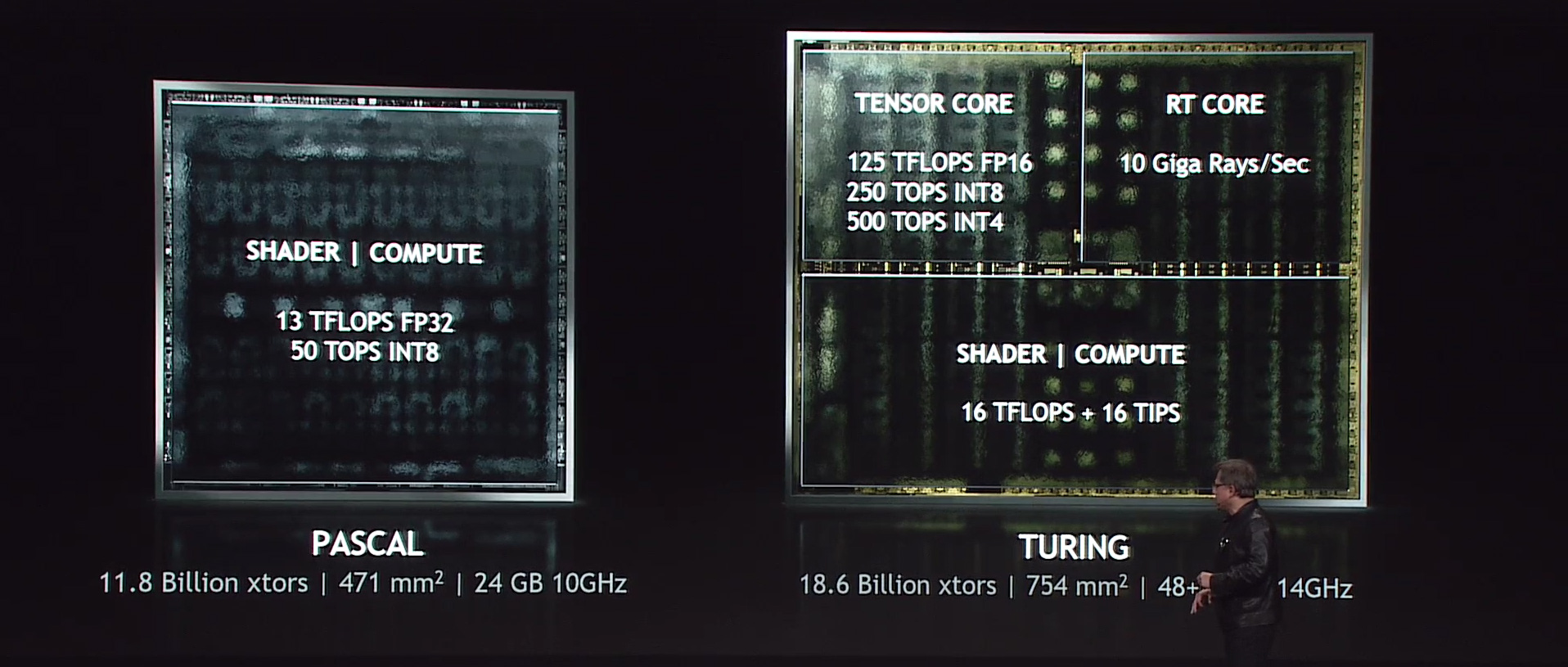
Along with the hardware specifications announced thus far, NVIDIA has also thrown out a handful of performance numbers for Turing hardware. It should be noted that there is a lot more we don’t know here than we do. However at a high level, these appear to be based around a mostly or completely enabled high-end Turing SKU featuring 4608 CUDA cores and 576 tensor cores. Clockspeeds are not disclosed, however as these numbers are profiled against Quadro hardware, we’re likely looking at lower clockspeeds than what we’ll see in any consumer hardware.
| NVIDIA Quadro Specification Comparison | ||||||
| RTX 8000 | GV100 | P6000 | M6000 | |||
| CUDA Cores | 4608 | 5120 | 3840 | 3072 | ||
| Tensor Cores | 576 | 640 | N/A | N/A | ||
| ROPs | 96? | 128 | 96 | 96 | ||
| Boost Clock | ~1730MHz? | ~1450MHz | ~1560MHz | ~1140MHz | ||
| Memory Clock | 14Gbps GDDR6 | 1.7Gbps HBM2 | 9Gbps GDDR5X | 6.6Gbps GDDR5 | ||
| Memory Bus Width | 384-bit | 4096-bit | 384-bit | 384-bit | ||
| VRAM | 48GB | 32GB | 24GB | 24GB | ||
| ECC | ? | Full | Partial | Partial | ||
| Half Precision | 32 TFLOPs? | 29.6 TFLOPs? | N/A | N/A | ||
| Single Precision | 16 TFLOPs | 14.8 TFLOPs | 12 TFLOPs | 7 TFLOPs | ||
| Double Precision | ? | 7.4 TFLOPs | 0.38 TFLOPs | 0.22 TFLOPs | ||
| Tensor Performance | 500 TOPs (INT4) |
119 TFLOPs (FP16) |
N/A | N/A | ||
| TDP | ? | 250W | 250W | 250W | ||
| GPU | Unnamed Turing | GV100 | GP102 | GM200 | ||
| Die Size | 754mm2 | 815mm2 | 471mm2 | 601mm2 | ||
| Transistor Count | 18.6B | 21.1B | 11.8B | 8B | ||
| Architecture | Turing | Volta | Pascal | Maxwell 2 | ||
| Manufacturing Process | TSMC 12nm FFN? | TSMC 12nm FFN | TSMC 16nm | TSMC 28nm | ||
| Launch Date | Q4 2018 | March 2018 | October 2016 | March 2016 | ||
Along with the aforementioned 10GigaRays/sec number for the RT cores, for the tensor cores NVIDIA is touting 500 trillion tensor operations per second (500T TOPs). For reference, NVIDIA frequently quotes the GV100 GPU as maxing out at 120T TOPs, however these are not the same. Specifically, while the GV100 was quoted with FP16 operations, Turing is being quoted with extremely low precision INT4, which just so happens to be one-quarter the size of FP16, and thus 4x the throughput. If we do normalize for precision, then Turing's tensor cores don't appear to have better throughput per core, but rather they offer more precision options than Volta did. At any rate, with 576 tensor cores in this chip is quite close to the 640 offered by GV100, but at the end of the day is still a lower amount.
As for the CUDA cores, NVIDIA is saying that the Turing GPU can offer 16 TFLOPS of performance. This is slightly ahead of the 15 TFLOPS single precision performance of the Tesla V100, or even a bit farther ahead of the 13.8 TFLOPS of the Titan V. Or if you’re looking for a more consumer-focused reference, it’s about 32% more than the Titan Xp. Some quick paper napkin math with these figures would put the GPU clockspeed at around 1730MHz, assuming there have been no other changes at the SM level which would throw off the traditional ALU throughput formulas.
Meanwhile NVIDIA has stated that the Quadro cards will come with GDDR6 running at 14Gbps. And with the top two Quadro SKUs offering 48GB and 24GB of GDDR6 respectively, we are almost looking at a 384-bit memory bus for this Turing GPU. By the numbers, this adds up to 672 GB/sec of memory bandwidth for both of the top two Quadro cards.
Otherwise with the architectural shift, it’s difficult to make too many useful performance comparisons, especially against Pascal. From what we’ve seen with Volta, NVIDIA’s overall efficiency has gone up, especially in well-crafted compute workloads. So the roughly 33% improvement in on-paper compute throughput versus the Quadro P6000 may very well be underestimating things. As for consumer product speculation, I’ll hold off on that entirely.
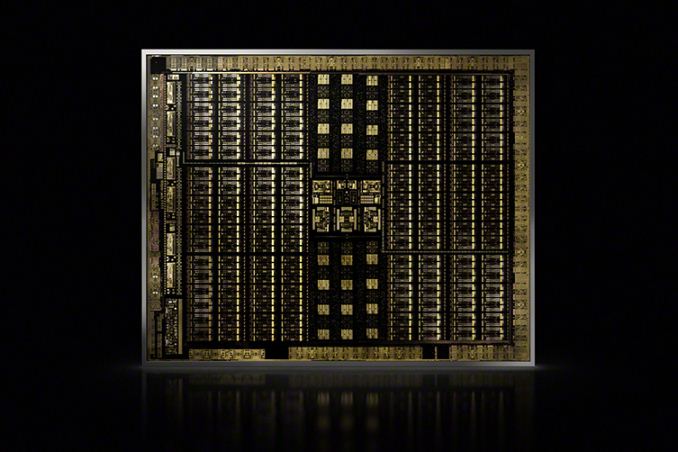
I'll also quickly touch upon the die size of this new GPU. At 754mm2 it's not just large, but it's huge. Compared to other GPUs it's second in size only to NVIDIA's GV100, which for now at least remains the NVIDIA flagship in certain respects. And with 18.6 billion transistors, it's easy to see why the resulting chip needed to be so big. Pardon the pun, but it's clear that NVIDIA has some very big plans for this GPU, and enough so that they can justify having two GPUs in their product stack that are so enormously large.
NVIDIA for their part hasn't stated the specific model number of this GPU – if it's the traditional 102-class GPU, or even the 100-class GPU. The sheer size of the GPU has me leaning towards the latter, but the matter is somewhat arbitrary at this point since the only thing even remotely comparable is GV100. Either way, it does have me wondering whether we're going to see this GPU filter down to consumer products in some form; it's so large that NVIDIA may intend to keep it for their more profitable Quadro and Tesla GPUs. In which case this specific GPU won't be what eventually hits consumer cards.
Coming in Q4 2018, If Not Sooner
Wrapping things up, alongside the Turing architecture announcement, NVIDIA has announced that the first 3 Quadro cards based on Turing GPUs – the Quadro RTX 8000, RTX 6000, and RTX 5000 – will be shipping in Q4 of this year. As the very nature of this reveal is somewhat inverted – normally NVIDIA announces consumer parts first – I wouldn’t necessarily apply that same timeline to consumer cards, which don’t have as stringent the validation requirements. Still, this means we’ll see Turing hardware in Q4 of this year, if not sooner. Interested Quadro buyers will want to start saving their pennies now: a top-tier Quadro RTX 8000 will set you back a cool $10,000.
Finally, as for NVIDIA’s Tesla customers, the Turing launch leaves Volta in a state of flux. NVIDIA has not told us whether Turing will eventually expand into the high-end Tesla space – replacing the GV100 – or if their one-off Volta part will remain the master of its domain for a generation. However as the other Tesla cards have been Pascal-powered thus far, they are very clear candidates for a Turing treatment in 2019.


83 Comments
View All Comments
tyger11 - Monday, August 13, 2018 - link
This is Turing; why would you even bring up gaming?mdriftmeyer - Monday, August 13, 2018 - link
He most likely brought it up as Nvidia has been touting the next advancement in gaming is a Real-Time Ray Tracing Graphics GPUs.inighthawki - Tuesday, August 14, 2018 - link
Turing is just the architecture name. I presume you mean that these are Quadro cards?tipoo - Monday, August 13, 2018 - link
Gaming event is next week, with the Geforce version maybe launching there.cmdrdredd - Monday, August 13, 2018 - link
Pretty much any new tech for game engines runs poorly on the first hardware. Tessellation wasn't that fast on the first GPUs that could do it, DX10/11/12 were all not that fast on first gen GPUs too.I think this will be no different.
Spunjji - Tuesday, August 14, 2018 - link
DX9 ran like stink on the Radeon 9700 Pro and DX12 showed significant gains on AMD's existing GCN hardware, so that comment only holds if you're limiting it to Nvidia chips. It's a trivial observation to say that second-gen performs better - it'd be an automatic failure if it didn't ;)somejerkwad - Tuesday, August 14, 2018 - link
The new Metro title has it and demonstrates an advantage for Titan V. FF15 also demonstrates a mild lead for Titan V vs 1080 ti which could possibly be related to the ray-tracing or another architectural advancement. They also showed off a live render Star Wars animation a while back. The hardware exists already for the higher end segments of the market and the software is coming along faster than it really should when considering that there's still no consumer market for the stuff, at least until nVidia stops holding out on us.Oxford Guy - Wednesday, August 15, 2018 - link
1) Sell to people with deep pockets. 2) Use e-peen features to get mindshare via reviewersAlistair - Monday, August 13, 2018 - link
Basically with Turing, what we know of as a GPU is changing quite a bit.Downside is so much money and die area spent without increasing performance in existing titles and engines. I'm not sure I want to pay double without seeing double performance in my existing titles, but today is marking the beginning of the transition to ray-tracing it seems.
Dr. Swag - Tuesday, August 14, 2018 - link
>implying these are meant for gamers, lolThese say quadro, not geforce. They're meant for professionals. I wouldn't be surprised if they released the geforce variants in a week or two without so much vram, disabled tensor cores, no ecc (not sure if the quadros do have it though), much lower double precision (these might support it at 1/2 or 1/3 rates), and perhaps less RT cores. Based on the die size of this monster, it most likely does have a lot of double precision hardware. In which case I'd expect nvidia to keep this massive 754 mm^2 die for quadros and teslas (and perhaps one Titan) and make a new die for geforce that should be a fair bit smaller.
You seem to think these prices are what the geforce cards will be. Just looking at the past these prices for quadros aren't completely out of the ordinary.