Investigating NVIDIA's Jetson AGX: A Look at Xavier and Its Carmel Cores
by Andrei Frumusanu on January 4, 2019 11:00 AM EST- Posted in
- NVIDIA
- SoCs
- Xavier
- Automotive
- Jetson
- Jetson AGX
Machine Inference Performance
The core aspects of the Xavier platform are its machine inferencing performance characteristics. The Volta GPU alongside the DLA core represent significant processing power in a compact and low-power platform.
To demonstrate the machine learning inference prowess of the system, NVIDIA provides the Jetson boards with a slew of software development kits as well as hand-tuned frameworks. The TensorRT framework in particular does a lot of heavy lifting for developers and represents the main API through which the GPU’s Tensor units as well as the DLA will be taken advantage of.
NVIDIA prepared a set of popular ML models for us to test out, and we’d be able to precisely configure the models in terms of how they were run on the platform. All the models running on the GPU and its Tensor core were able to run at either quantized INT8 forms, or in FP16 or FP32 forms. The batch sizes were also configurable, but we’ve kept it simple at just showcasing the results with a batch size of 32 images as NVIDIA claims this is the more representative use-case for autonomous machines.
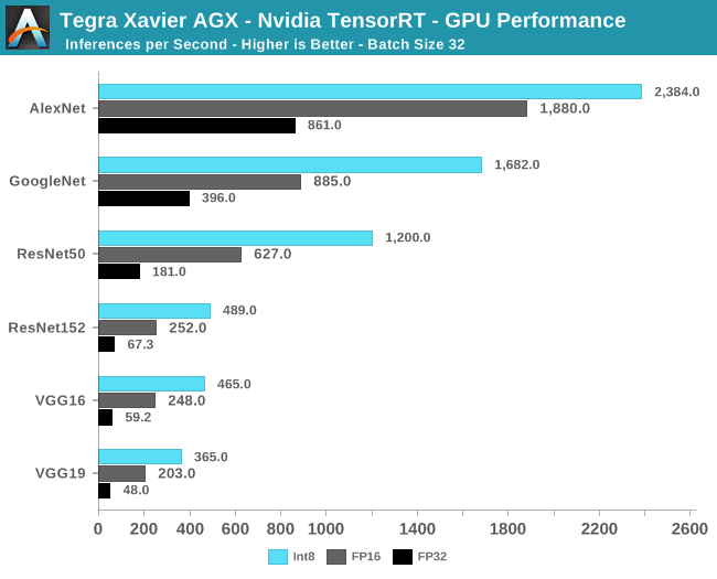
The results of the GPU benchmarks are a bit esoteric because we have few comparison points against which we can evaluate the performance of the AGX. Among the more clear results we see here is that the inferencing performance in absolute terms is reaching rather high rates, particularly in the INT8 and FP16 modes, representing sufficient performance to run a variety of inferencing tasks on a large number of input sets per second. The only real figure we can compare to anything in the mobile market is the VGG16 results compared to the AImark results in our most recent iPhone XS review, where Apple’s new NPU scored a performance of 39 inferences/second.
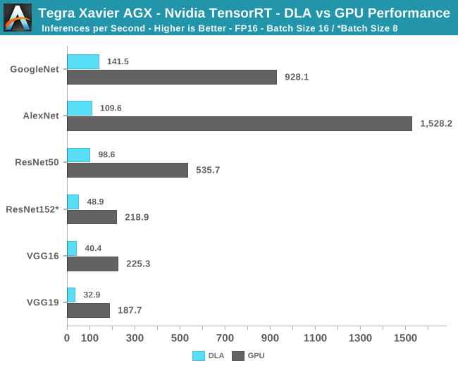
NVIDIA also made it possible to benchmark the DLA blocks, however this came with some caveats: The current version of the TensorRT framework was still a bit immature and thus doesn’t currently allow for running the models in INT8 mode, forcing us to resort to comparisons in FP16 mode. Furthermore I wasn’t able to run the tests with the same large batch size as on the GPU, so I’ve reverted to using smaller sizes of 16 and 8 where appropriate. Smaller batch sizes have more overhead as it takes proportionally longer time on the API side of things and less actual processing time on the hardware.
The performance of the DLA blocks at first glance seems a bit disappointing, as their performance is just a fraction of what the Volta GPU is able to showcase. However raw performance isn’t the main task of the DLA, it serves as a specialized offloading block which is able to operate at higher efficiency points than the GPU. Unfortunately, I wasn’t able to directly measure the power differences between the GPU and the DLA, as introducing my power measurement equipment into the DC power input of the board led to system instabilities, particularly during the current spikes when the benchmarks were launching their workloads. The GPU inference workloads did see the board power reach around ~45W while in its peak performance mode.
NVIDIA's VisionWorks Demos
All the talk about the machine vision and inferencing capabilities of the platform can be something that’s very hard to grasp if you don’t have a more intimate knowledge of the use-cases in the industry. Luckily, NVIDIA’s VisionWorks SDK comes with a slew of example demos and source code projects that one can use as a baseline for one’s commercial applications. Compiling the demos was a breeze as everything was set up for us on the review platform.
Alongside the demo videos, I also opted to showcase the power consumption of the Jetson AGX board. Here we’re measuring the power of the platform at the 19V DC power input with the board at its maximum unlimited performance mode. I had board’s own fan disabled (it can be annoyingly loud) and instead used an externally-powered 120mm bench fan blowing onto the kit. At a baseline power level, the board used ~8.7-9W while sitting idle and actively outputting to a 1080p screen via HDMI while also being connected to Gigabit Ethernet.
The first demo showcases the AGX’s feature tracking capabilities. The input source is a pre-recorded video to facilitate testing. While the video output was limited to 30fps, the algorithm was running in excess of 2-300fps. I did see quite a wide range of jitter in the algorithm fps, although this could be attributed to scheduling noise due to the low duration of the workload while in a limited FPS output mode. In terms of power, we see total system consumption hover around 14W, representing an active power increase of 5W above idle.
The second demo is an application of a Hough transform filter which serves as a feature extraction algorithm for further image analysis. Similarly to the first demo, the algorithm can run at a very high framerate on a single stream, but usually we’d expect a real use-case to use multiple input streams. Power consumption again is in the 14W range for the platform with an average active power of ~4.5W.
The motion estimation demo determines motion vectors of moving objects in a stream, a relatively straightforward use-case in automotive applications.
The fourth VisionWorks demo is the computational implementation of EIS (Electronic image stabilisation), were given an input video stream the system will crop out margins of the frame and use this space as the stabilisation window in which the resulting output stream will be able to elastically bounce against, reducing smaller juddery motions.
Finally, the most impressive demo which NVIDIA provided was the “DeepStream” demo. Here we see a total of 25 720p video input streams played back all simultaneously all while the system is performing basic object detection in every single one of them. This workload represented a much more realistic heavy use-case being able to take advantage of the processing power of the AGX module. As you might expect, power consumption of the board also rose dramatically, averaging around 40W (31W active work).


51 Comments
View All Comments
linuxgeex - Friday, November 8, 2019 - link
Add this line to the following files (linux/bsd or windows)/etc/hosts or c:/windows/system32/driver/hosts
127.0.0.1 ads.servebom.com
job done.
TheinsanegamerN - Friday, January 4, 2019 - link
auto video ads are hell incarnate.Yojimbo - Friday, January 4, 2019 - link
Regarding NVIDIA's future CPU core development, I think it's important to note that NVIDIA has developed all major IP blocks on the SoC. That probably allows them to work on integration sooner than if they relied on externally developed IP blocks. Also, they have the ability to tune their cores and fabric to their intended application, which is a narrow subset of what ARM is developing for. I'm guessing NVIDIA doesn't tune the performance of their CPU cores using specint or specfp. They probably look at much more specific and realistic benchmarks.And by the time the Cortex A76AE is available for NVIDIA to use they will probably have a next iteration of their CPU which perhaps will show up in Orin in early 2021 or even late 2020. It's not clear to me what delayed Xavier from NVIDIA's original schedule. It's possible they'll be able to get the next one out with less time between the launch of the underlying GPU architecture and the availability of the SoC. There was a lot of new stuff that went into Xavier other than the GPU architecture, such as the increased safety features, the DLA, and the PVA.
DeepLearner - Friday, January 4, 2019 - link
I hope they'll send you a T4 soon! I'm dying for numbers on those.eastcoast_pete - Friday, January 4, 2019 - link
@Andrei: thanks for this review. I wonder if the recent loss of a larger client in the automotive sector (Audi/Volkswagen) to Samsung played a role in Nvidia's willingness to make samples available to you for review. As of model year 2021, Audi will stop using Tegra-based units and move to Samsung's Exynos Auto V9 SoC, which actually features an 8 A76 cores based on ARM's A76 AE design for automotive/vehicular use.While that specialized SoC is still awaiting mass production, I also wonder if Samsung's choice to use straight-up ARM A76 cores (yes, they are AE, so not standard A76) portends a sea change for the mainstream Exynos lines also? As you pointed out, Mongoose turned out to be quite disappointing, so is there a change coming? Would appreciate your insights and comment!
webdoctors - Friday, January 4, 2019 - link
I was also confused by the news of Audi using Samsung chips. I don't think this changes the Audi/Nvidia relationship from googling: http://fortune.com/2017/01/05/audi-nvidia-2020/I think in the infotainment sector there's just a lot of competition for cheap chips and a low bar for entry. Any Mediatek or run of the mill cellphone chip should do. I doubt you'd care about ECC or safety in the HW playing your music or watching movies. My current car has an aftermarket unit that's 10 years old that can play DVD movies, has GPS maps and integrates a backup camera.
I'm not sure how you'd program a beast of a chip here, or even what the right benchmarks are since you wouldn't need it just play movies, show maps or run CPU benchmarks. With all the inferencing and visual processing it'd be a waste of resources and money to use it for the traditional tasks done today in cars.
I'm really curious how Anandtech evaluates these specialized products that aren't your run of the mill CPU/GPU/HDD.
unrulycow - Saturday, January 5, 2019 - link
This is obviously overkill for the entertainment system. It's main purpose is for the semi-autonomous driving systems like Cadillac's SuperCruise or Tesla's Autopilot.Andrei Frumusanu - Friday, January 4, 2019 - link
As far as I know their mobile roadmap still uses custom cores, there's probably different requirements for automotive or they could have simply said that 8 A76s make a lot more sense than 8 custom cores.eastcoast_pete - Saturday, January 5, 2019 - link
Thanks Andrei! Yes, design requirements for automotive/vehicle-embedded are different in key areas (safety/security). However, I was/am struck by Samsung not adapting their own Mongoose design for AE use. Maybe their client (Audi) preferred the stock A76 AE design, and it wasn't economical to adapt Mongoose. However, this now means that the most powerful Samsung SoC design (A76 octacore) might be found in - Audi cars.unrulycow - Saturday, January 5, 2019 - link
They are also losing Tesla as a client. Tesla decided to create their own chip which will theoretically start going into cars in Q2. I would love to see a comparison between the two chips.