The AMD Radeon VII Review: An Unexpected Shot At The High-End
by Nate Oh on February 7, 2019 9:00 AM ESTVega 20 Under The Hood: GCN on 7nm
Though we’ve known of Vega 20 for some time with the launch of server-class Radeon Instinct MI50 and MI60, its arrival to the consumer space does mark the first 7nm gaming card. Rapidly moving down to a lower node – this time from GlobalFoundries 14nm LPP to TSMC 7nm (CLN7FF) – used to be an AMD/ATi hallmark, and once again AMD is pushing the envelope by bringing it so early to consumers. That being the case, all the attributes of Vega 20 look squarely to be for the professional/server crowd, though not devoid of benefits for gaming.
Of the many threads in the Radeon VII story, the fate of Vega as a whole has been nothing short of enigmatic. To start things off, the 7nm Vega 20 GPU making its way to consumers was a surprise to most, at least arriving this early. And while AMD only made mention of Vega 20 in reference to Radeon Instinct products – referring to the forthcoming Navi when speaking about 7nm GPUs for gamers – AMD now maintains that the plan was always to bring Radeon VII to market. Perhaps the same might have been said regarding Vega on 14nm+/12LP and the Vega 11 GPU (not to be confused with Ryzen 2400G’s 11 Vega compute units), though to be clear this is hardly unusual given the nature of semiconductor development.
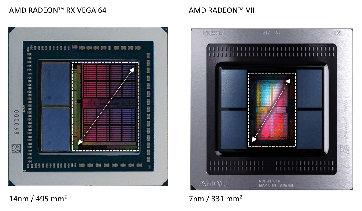
To be fair, AMD has only been coy at best about Vega since the RX Vega launch, which didn’t quite land where AMD wanted it to. But even as a bit of Schrodinger’s silicon, the existence of Radeon VII does raise some interesting questions about 7nm. For one, AMD had already moved up their Vega 20 sampling and launch windows previously. So Radeon VII’s launch timing is realistically the earliest it could be for a consumer derivative of the Radeon Instinct. Even more so is that with a die size of 331mm2, these aren’t small mobile SoCs or comparable ‘pipecleaner’ silicon that we’ve seen so far on TSMC 7nm. Designed with compute/ML-oriented enhancements, equipped with 4 HBM2 stacks, and fabbed on a maturing and cutting-edge 7nm node, Vega 20 has nothing on paper to push for its viability at consumer prices. And yet thanks to a fortunate confluence of factors, here we are.
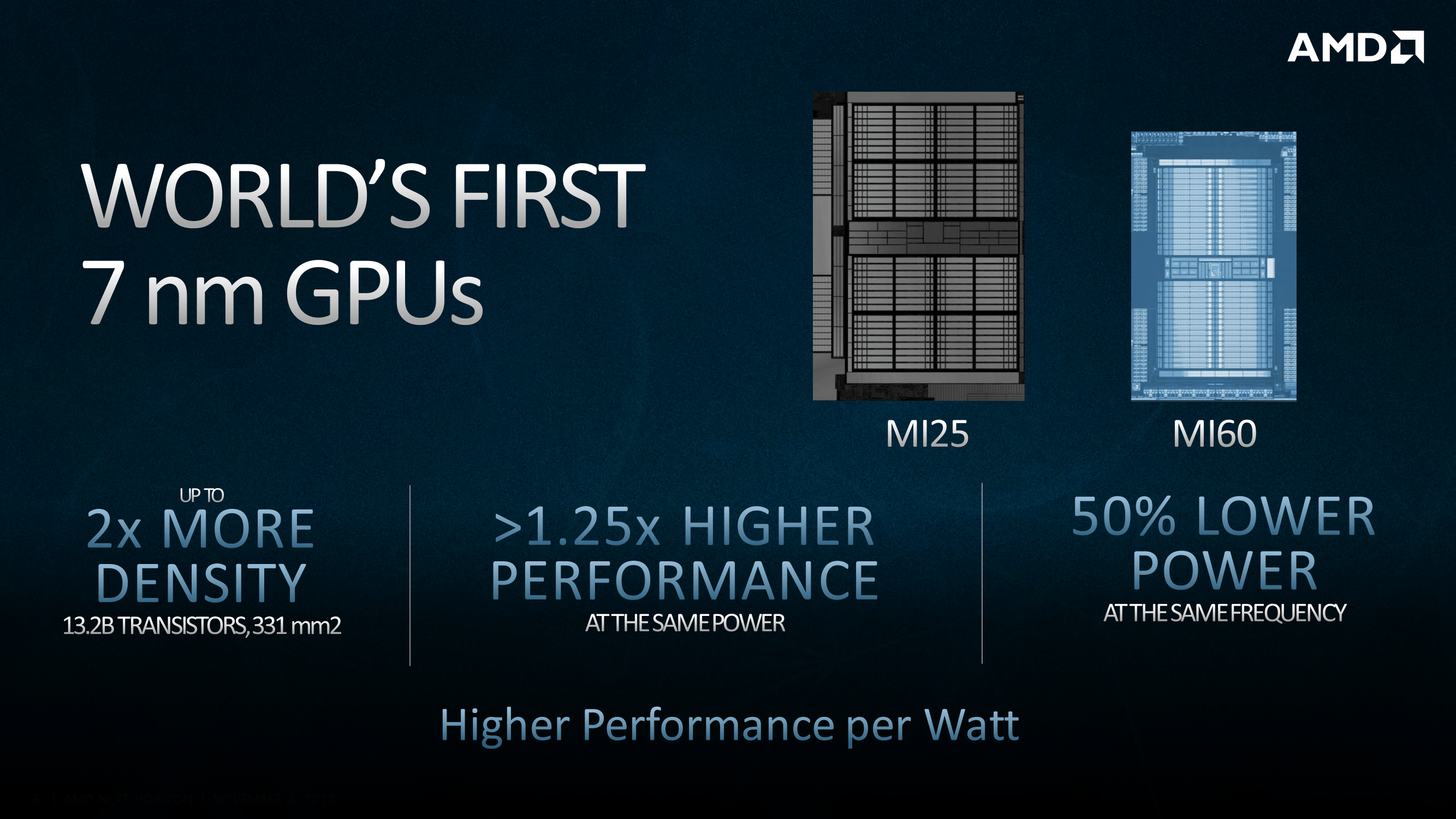
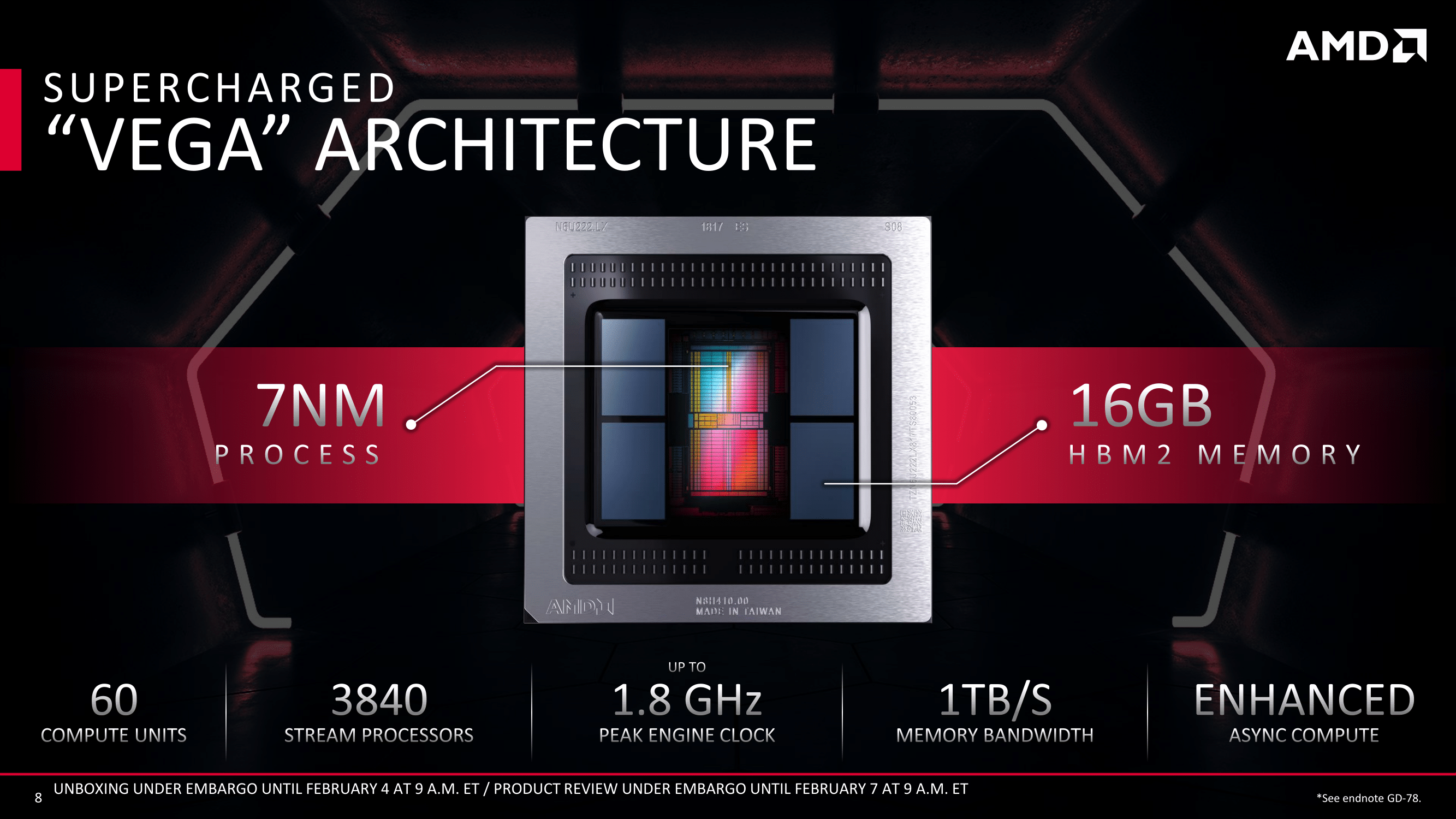
At a high level. Vega 20 combines an updated GCN 5 architecture with a 7nm process, coming out to 13.2B transistors on 331mm2 (versus 12.5B transistors on 496mm2 for Vega 10). Typically with die shrinks, these space-savings are often reinvested into more transistors – for a gaming card, that can mean anything from more CUs and functional blocks, to layout redesigns and hardened data paths for improved frequency tolerance. The latter, of course, is to enable higher clockspeeds, and this design choice was a big part of Vega 10, where a significant number of transistors were invested to meeting the requisite timing targets. In conjunction with power-savings of a smaller node, a chip can then get to those higher clocks without additional power.
For Vega 20 however, much of the saved space was left simply as that: more space. There’s several reasons of this, some obvious, and some less so. To start things off, as a relatively large high-performance GPU on a leading-edge 7nm node early in its life, development and production is already costly and likely lower-yielding, where going any larger would cost substantially more and yield less. And though TSMC’s 7nm process has only publicly been seen in mobile SoCs thus far, Vega 20 presumably makes good use of the HPC-oriented 7.5T libraries as needed, as opposed to using the 6T libraries intended for mobile SoCs.
But more importantly, the saved space allows room for two more stacks of HBM2 on a similarly-sized interposer. For current-generation HBM2 densities and capabilities, the limit for a two stack chip is 16GB of memory, using a pair of "8-Hi" stacks. But for a server-grade GPU – especially one targeting machine learning – a four stack configuration needed to happen in order to allow for 32GB of memory and a wider 4096-bit bus. For Vega 20, AMD has delivered on just this, and furthermore is producing both 32GB (8-Hi) and 16GB (4-Hi) versions of the chip.
Radeon VII, in turn, is tapping one of these 16GB chips for its core design. It should be noted that this isn't AMD's first 16GB Vega card – they also produced one early on with their early-adopted focused Vega Frontier Edition card – but since the Frontier Edition's retirement, this is the first (re)introduction of a 16GB card to AMD's Vega lineup.
Going with a 16GB for a consumer(ish) card is a bit of a gamble for AMD. And, I suspect, this is part of the reason we're also seeing AMD chase part of the professional visualization market with the Radeon VII. When it comes to workstation use and content creation tasks, more VRAM is an easy sell, as there are already datasets that can use all of that VRAM and more. But for gaming this is a harder sell, as games have more fixed VRAM requirements, and absent such a large card until now, developers haven't yet started targeting 16GB cards. On the flip side, however, the statement "this card has more than enough VRAM" has proven to be famous last words, and in 2019 a flagship enthusiast-grade gaming card ought to have that much anyway.
Getting back to Vega 20's design then, the other step AMD has taken to reduce the complications and cost of 7nm is by sticking to a die-shrink of a known architecture. Here AMD has added optimizations over Vega 10, but they did not risk a large redesign. Basically it's the logic behind the ‘tick’ of Intel’s old ‘tick-tock’ strategy.
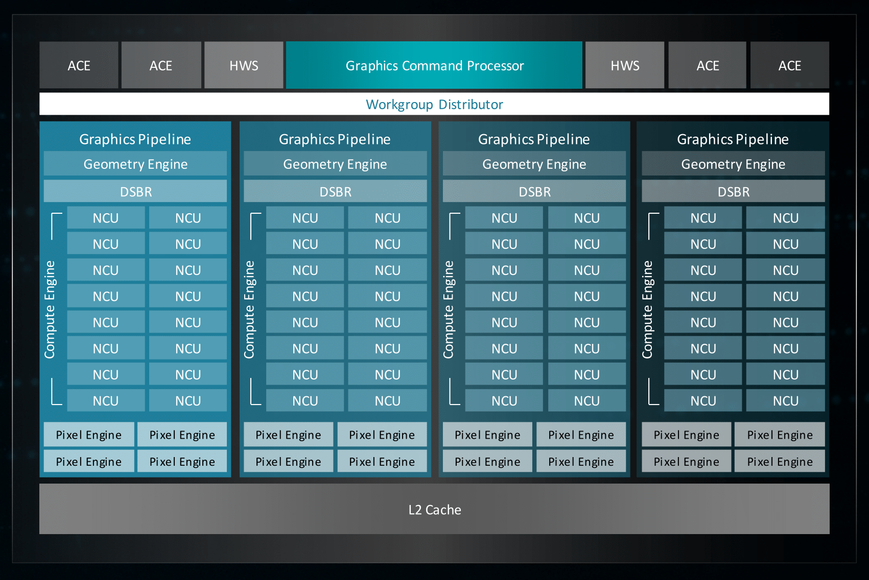
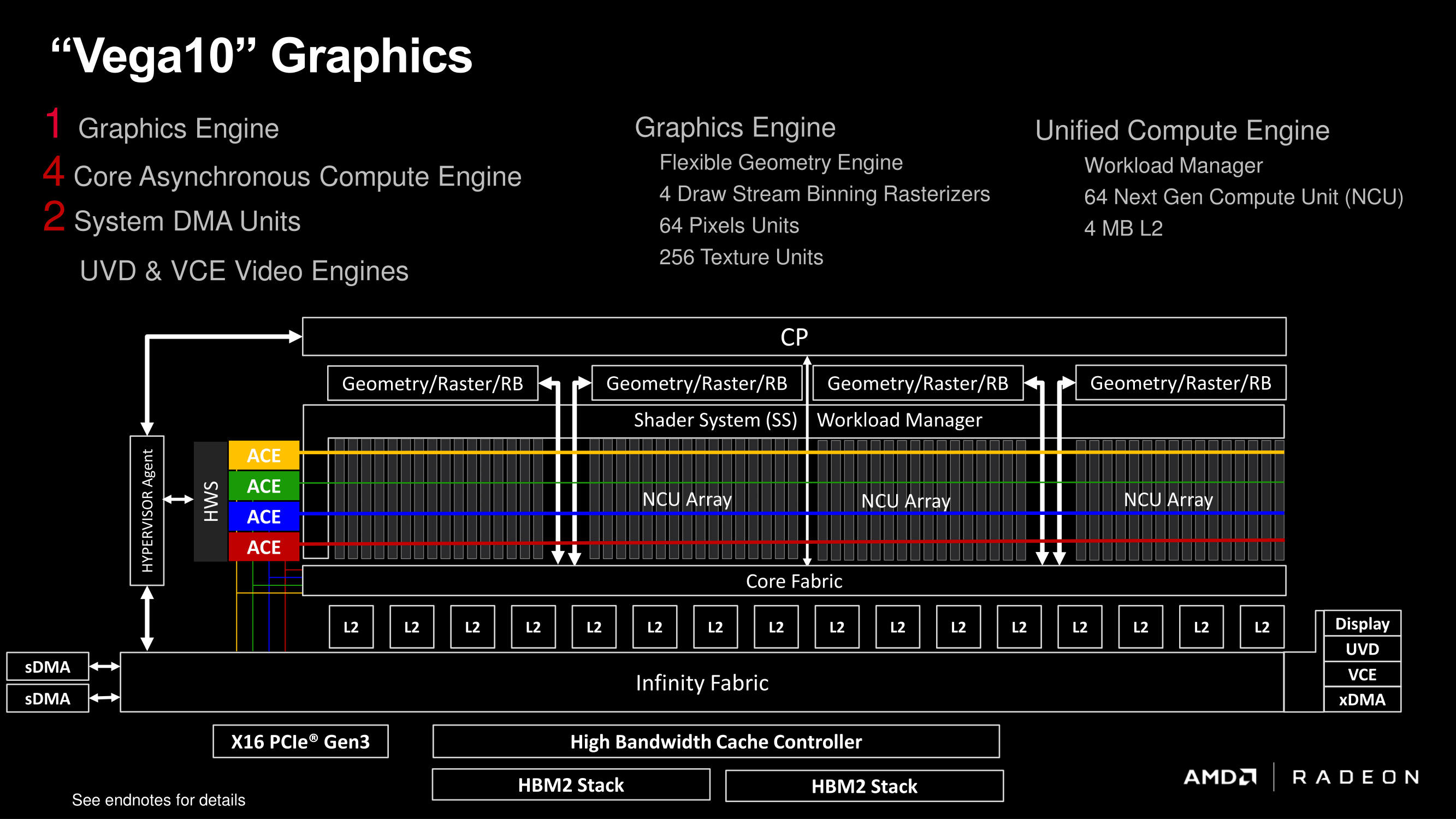
In fact Vega 20 is such a straightforward shrink of Vega 10 in this manner that, outside of the number of memory controllers, all of the other functional unit counts at the same. The GPU packs 64 CUs and 256 texture units segmented into 4 Shader Engines, which in turn are paired with 64 ROPs and AMD's multi-queue command processor.
(I should add that by going this route, AMD also neatly sidesteps the question of shader engine scaling. The nature of that 4 SE limitation has been left vague in recent years, but with Vega there were hints of a path beyond with improved load-balancing via the intelligent workgroup distributors (IWD). Regardless, it would be a complex task in itself to tweak and redesign a balanced 4+ SE configuration, which might be unnecessary effort if AMD has fundamental changes to GCN in the pipeline.)
So on an architectural level, Vega 20 is very much an evolutionary design. But with that said, there is a bit more evolution to it than just the die-shrink, the combination of which means that Vega 20 should in practice be a bit faster than Vega 10 on a clock-for-clock basis.
The big improvement here is all of that extra memory bandwidth; there's now over twice as much bandwidth per ROP, texture unit, and ALU as there was on Vega 10. The bodes particularly well for the ROPs, which have traditionally always been big bandwidth consumers. Not stopping there, AMD has also made some improvements to the Core Fabric, which is what connects the memory to the ROPs (among other things). Unfortunately AMD isn't willing to divulge just what these improvements are, but they have confirmed that there aren't any cache changes among them.
Another piece of the puzzle is that AMD has added some new instructions and data types that will speed up machine learning in certain cases. AMD hasn't given us the complete details here, but at a high level we know that they've added support for INT8 and INT4 data types, which are useful for some low-precision inference scenarios. AMD has also added a new FP16 dot product that accumulates as an FP32 result, a rather specific scenario that is helpful for some machine learning algorithms, as it produces a higher precision result than a FP16-in/FP16-out dot product.
Speaking of data types, AMD has also significantly ramped up their FP64 performance for Vega 20. As a core architecture, GCN allows a GPU to be built with a rate ranging from 1/2 to 1/16 the FP32 rate. For pure consumer GPUs this has always been 1/16, however for GPUs that have pulled double-duty as server-focused chips, they have enabled 1/4 and 1/2 rates in the past. Vega 20, in turn, is the first 1/2 rate FP64 GPU from AMD since Hawaii in 2013. This means that while its general FP32 performance gains over Vega 10 cards are somewhat limited, its FP64 gains are nothing short of massive – better than 8x over the RX Vega 64, on paper. Of course as a consumer card the Radeon VII doesn't quite get to enjoy these benefits – it's limited to 1/4 rate – but more on that later.
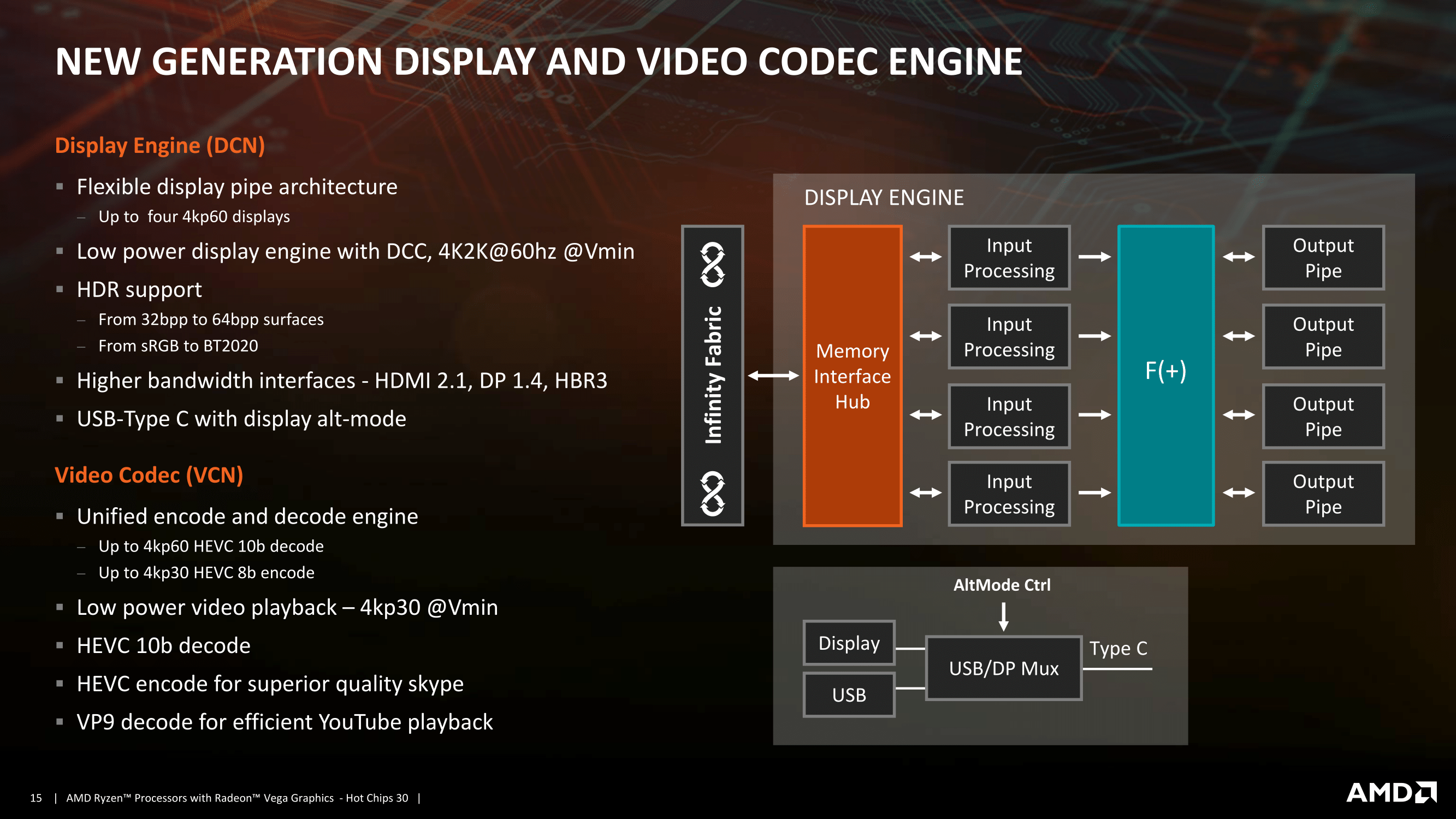
Meanwhile, for AMD's video and display controller blocks, there have only been minor, incremental updates. Officially, the display controller (DCE) is up to version 12.1, while we're on unified video decoder (UVD) 7.2, and video coding engine (VCE) 4.1. No additional encoding or decoding feature support have been added compared to Vega 10. For what it’s worth, we’ve already seen the successor blocks with Raven Ridge’s Display Core Next and Video Core Next 1.0, so this may be the last architecture that those ASICs grace us with their presence.
Wrapping up the functional blocks is a new style of SMU, discussed in recent Linux kernel patches. Orthogonal, but closely related, is improved thermal monitoring, where the number of temperature diodes has been doubled to 64 sensors. As a consequence, AMD is now fully utilizing junction temperature monitoring instead of edge temperature monitoring. Junction temperature measurements were used in Vega 10 (showing up as ‘hotspot’ temperature) but Vega 20 has made the full jump to junction temperature for the full suite of fanspeeds, clockspeeds, and such. The result is more accurate reporting, as well as minor 1-2% performance gains (via reduced throttling) that AMD cites from internal testing.
The updated SMU also brings with it a knock-on effect: temperature, clockspeed, and related GPU metrics are no longer read through registers, but instead grabbed straight from the SMU. Naturally, this breaks compatibility with third-party utilities (i.e. GPU-Z), and while AMD has already notified some developers of these changes, applications will still need to be updated to use AMD's new API calls.
Finally, as this is AMD's first new high-end Vega silicon since the original Vega 10 in 2017, there have been a few questions swirling around Vega’s forward-looking hardware features. AMD's communication hasn't always been clear here, and as a result these features have become sort of a perpetual source of consumer confusion.
To settle matters for Vega 20 then, AMD doesn’t seem to be changing the situation here. Which is to say that there have been no further developments as far as AMD's primitive shaders are concerned. Primitive shaders will still require explicit developer support – something AMD has not enabled – and so the full capabilities of Vega 20's Next-Gen Geometry path aren't being utilized (though we should note that the Intelligent Workgroup Distributor portion has always been enabled).
Meanwhile, AMD's Draw Stream Binning Rasterizer (DSBR) was already up and working in Vega 10, so this hasn't changed; the feature is enabled for an unspecified list of games. And checking in quickly on Rapid Packed Math (fast FP16), this is in use for two known games: Far Cry 5 and Wolfenstein II.


289 Comments
View All Comments
zodiacfml - Friday, February 8, 2019 - link
The first part of your conclusion describes what this product is. It is surprising to see this card's existence at 7nm, a Vega with 16GB of HBM2.It appears to me that AMD/TSMC is learning the 7nm process for GPUs/CPUs and the few chips they produce be sold as a high end part (as the volume/yields is being improved).
AMD really shot high with its power consumption (clocks) and memory to reach the pricing of the GTX 2080.
However, I haven't seen a publisher to show undervolting results. Most Vegas perform better with this tweak.
Samus - Saturday, February 9, 2019 - link
I think you are being a little too critical of this card. Considering it’s an older architecture, it’s impressive it’s in the 2080’s ballpark.And for those like me that only care about Frostbite Engin based games, this card is obviously a better option between the two cards at the same price.
You also ignored the overclockong potential of the headroom given by moving to 7nm
D. Lister - Saturday, February 9, 2019 - link
"You also ignored the overclockong potential of the headroom given by moving to 7nm"Unfortunately it seems to be already overclocked to the max on the core. VRAM has some headroom but another couple of hundred MHz isn't going to do wonders considering the already exorbitant amount available.
D. Lister - Saturday, February 9, 2019 - link
*...considering the already exorbitant amount [of bandwidth] available.Oxford Guy - Saturday, February 9, 2019 - link
"I think you are being a little too critical of this card."Unless someone can take advantage of the non-gaming aspects of it, it is dead in the water at the current price point. There is zero reason to purchase a card, for gaming only, that uses more power and creates vastly more noise at the same price point of one that is much more efficient for gaming purposes. And, the only way to tame the noise problem is to either massively undervolt it or give it water. Proponents of this GPU are going to have to show that it's possible to buy a 3 slot model and massively undervolt it to get noise under control with air. Otherwise, the claim is vaporware.
Remember this information? Fiji: 596 mm2 for $650. Vega 10 495 mm2 for $500. Vega 20 331 mm2 for $700.
Yes, the 16 GB of RAM costs AMD money but it's irrelevant for gaming. AMD not only gave the community nearly 600 mm2 of chip it paired it with an AIO to tame the noise. All the talk from Su about improving AMD's margins seems to be something that gamers need to stop lauding AMD about and starting thinking critically about. If a company only has an inferior product to offer and wants to improve margins that's going to require that buyers be particularly foolish.
Samus - Sunday, February 10, 2019 - link
I wouldn't call the 16GB irrelevant. It trumps the 2080 in the two most demanding 4K titles, and comes relatively close in other ultra high resolution benchmarks.It could be assumed that's a sign of things to come as resolutions continue to increase.
Oxford Guy - Sunday, February 10, 2019 - link
"It could be assumed that's a sign of things to come as resolutions continue to increase."Developers adapt to Nvidia, not to AMD. That appears to be why, for instance, the visuals in Witcher 3 were watered-down at the last minute — to fit the VRAM of the then standard 970. Particularly in the context of VRAMgate there was an incentive on the part of Nvidia to be certain that the 970's VRAM would be able to handle a game like that one.
AMD could switch all of its discreet cards to 32 GB tomorrow and no developers would bite unless AMD pays them to, which means a paucity of usefulness of that 32 GB.
BenSkywalker - Saturday, February 9, 2019 - link
This offering is truly a milestone in engineering.The Radeon VII has none of the RTX or tensor cores of the competition, uses markedly more power *and* is built with a half node process advantage and still, inexplicably, is slower than their direct competitor?
I've gone back and looked, I can't find another example that's close to this.
Either TSMC has *massive* problems with 7 nm or AMD has redefined terrible engineering in this segment. One of those, at least, has to be at play here.
Oxford Guy - Saturday, February 9, 2019 - link
The RTX and Tensor die area may help with power dissipation when it's shut down, in terms of hot spot reduction for instance. Vega 20 is only 331 mm2. However, it does seem clear enough that Fiji/Vega is only to be considered a gaming-centric architecture in the context of developers creating engines that take advantage of it, à la DOOM.Since developers don't have an incentive to do that (even DOOM's engine is apparently a one-off), here we are with what looks like a card designed for compute and given to gamers as an expensive and excessively loud afterthought.
Oxford Guy - Saturday, February 9, 2019 - link
There is also the issue of blasting clocks to compensate for the small die. Rip out all of the irrelevant bits and add more gaming hardware. Drop the VRAM to 8 GB. Make a few small tweaks to improve efficiency rather than just shrink Vega. With those things done I wonder how much better the efficiency/performance would be.