ChipRebel Releases Exynos 9820 Die Shot: M4 CPUs in New Cluster
by Andrei Frumusanu on March 9, 2019 3:30 AM EST- Posted in
- Smartphones
- Samsung
- Mobile
- SoCs
- ChipRebel
- Exynos 9820
Every time a new SoC comes one, the one thing we eagerly await is for someone to release a die shot of the new chip. This process is most interesting when the new chip either comes with a new microarchitecture or a new process node. Last November, we covered the release of ChipRebel’s Kirin 980 die shot which gave us the first ever look of Arm’s new Cortex A76 CPU as well as Mali G76 GPU on a new 7nm process node.
The folks over there are at it again and have seemingly been very busy overnight, this time around tearing down the Galaxy S10 with the new Exynos 9820. I’ve been going back and forth with the ChipRebel team on these last two projects and they’re great guys, definitely visit them if you are in need of die shots.
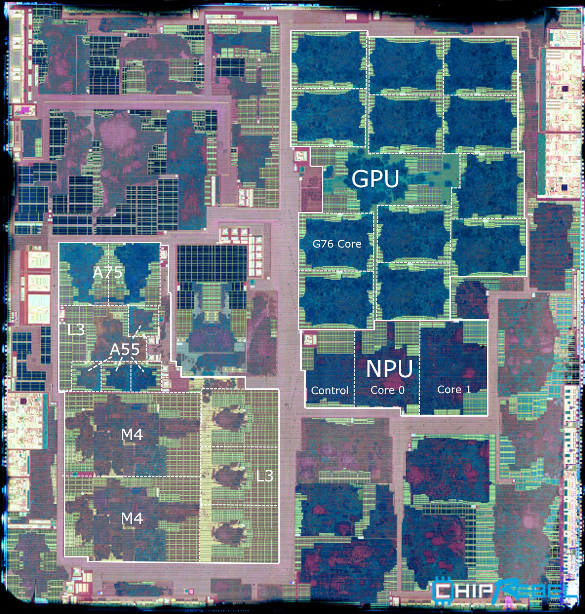
Die shot: Chip Rebel - Annotations/labelling: Andrei @ AnandTech
8nm not as small as 7nm
The first thing standing out for the Exynos 9820 is the fact that at ~127mm², the chip has actually grown compared to the 10LPP Exynos 9810 of last year. Samsung’s 8LPP node isn’t as aggressive in scaling as TSMC’s 7nm process, and in theory the process node should bring a conservative 15% reduced area compared to its preceding node, leaving TSMC at a notable density advantage this generation. Compared to the Kirin 980 at 74.13mm², the Snapdragon 855 at 73.27mm² and even Apple’s A12 at 83.27mm², the new Exynos 9820 clearly stands out as out of line compared to the competition.
The Exynos 9820 also changes a lot internally, compared to the Exynos 9810 last year. First off we notice that the CPU cluster isn’t as prominent as it was last year. The reason for this is simply that Samsung opted to only employ two of its new generation M4 cores as opposed to the quad-core layout of the M3 in the 9810.
Interesting in the die shot is the new cluster layout: Next to the M4 cores we see now three L3 slices with a similar design as we saw in the 9810. However north of the two M4 cores we see a further L3 slice that differs from the other three. This slice seems to be the one that connects the new Cortex A55 and A75 cores to Samsung’s cluster.
I’ve had the Galaxy S10+ with the Exynos 9820 in-house since yesterday, and I can confirm that the L3 cache has remained at a total of 4MB, although I need a bit more time to figure out exactly how much of this is accessible by the Cortex cores as there’s power management policies coming into play.
The important thing to note here is that the Cortex A55 cores are no longer handicapped by not sharing the same higher level cache hierarchy as the rest of the CPU complex.
The new Exynos M4 cores clock up to 2.73GHz, the A75 cores at up to 2.31GHz and the A55 cores up to 1.95GHz.
On the GPU side of things, we still see Samsung dedicate a lot of area to the Mali G76MP12 – although it’s doesn’t look as big as last year’s G72MP18.
Finally, below the GPU, we find Samsung’s new NPU. This is a dual-core design running at up to 933MHz and offering up to 1.9TOPs at 8-bit precision, although Samsung looks to be counting 6.9TOPs in quantised models. Samsung themselves publish the die area of this block to be 5.5mm².
We thank the guys at ChipRebel for sharing this die shot with the public as it offers great analysis of Samsung’s new chip! On our side, we have the S10+ in-house now and I’ll be working on the full detailed device+SoC review.


66 Comments
View All Comments
Fergy - Sunday, March 10, 2019 - link
@kaspar737 A76 is much larger than A75. They are a nice midway point between tiny A55 and huge M4Wilco1 - Sunday, March 10, 2019 - link
Certainly not - in the link below we have A76 = 3.5x A55. From this die photo we have A75 = 4x A55, M4 = 13.5x A55. Different processes of course, but A76 is not much larger.https://www.anandtech.com/show/13564/chiprebel-rel... we
anonomouse - Sunday, March 10, 2019 - link
This may not be a like for like comparison though, because the A55s in Kirin/Snapdragon have the L2, whereas these most likely do not - and the L2 is going to a significant fraction of the area for an A55.Wilco1 - Monday, March 11, 2019 - link
That's possible indeed. However the process makes a huge difference. SRAM seems to have terrible density on the 8nm process. Check how large each 1MB L3 slice is in 9820, larger than an A75, but on Kirin 980 a 2MB L3 slice easily fits in a A76...anonomouse - Tuesday, March 12, 2019 - link
That’s also a bit tough to say. We know the A76 is for sure larger than an A75 iso-process, and the A76s on the Kirin 980 have 512KB L2s. It’s not quite clear if the A75s on the 9820 have L2s either. From the die photo I suspect that they do not, but even if they do it doesn’t seem like it could be larger than 128KB from the arrangement of obvious macros of different sizes. Also note that the data arrays of the Exynos L3 slices are only about half the area of the entire slice, so that’s not quite the right comparison either as far as sram density.I should be clear though, none of this is to contest the point that the M4s seem ludicrously large in area for the performance they deliver. With that point, I fully agree. I’d probably ballpark the A76+512KB L2 at roughly being somewhere just a bit north of half the size of the M4 iso-process.
abufrejoval - Thursday, March 14, 2019 - link
Since Samsung most likely won't answer this directly, we can only speculate.Using the top-of-the-line A76 would have made the M4 more pointless for starters.
Then translating a design to a process is a significant effort. In some cases ARM will do the work, e.g. for a major node on TSMC. With Samsung 8nm, Samsung would have to do that themselves and they may not want to pay for that with every architecture ARM sells, unless it's the key selling point.
Also Samsung still has to pay per instance licenses for ARM cores and A75 is most likely cheaper than A76, while the A55 (or any secondary cores) costs almost nothing, when you've already paid for the A75.