Japan Display Develops 1.6-Inch Micro LED Display Module: 265 PPI & 3,000 Nits
by Anton Shilov on December 2, 2019 4:00 PM EST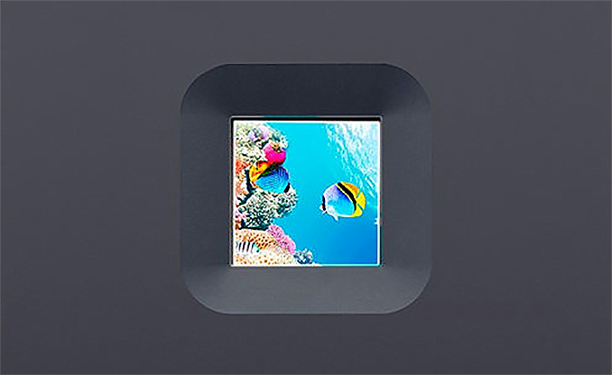
Japan Display Inc. (JDI) announced this week that it has completed development of its first Micro LED module. The prototype of the Micro LED module, which is a potential building block for next generation displays and TVs, offers a 265 PPI pixel density. JDI will be demonstrating the module at Fintech Japan 2019 later this week.
JDI’s Micro LED display prototype is a square module with a 1.6-inch diagonal, and offers a resolution of 300×300 pixels along with a maximum brightness of 3,000 nits. The prototype uses gallium nitride LED chips developed by glo (a Micro LED pioneer) and JDI’s LTPS backplane.
| JDI's Micro LED Display Module Prototype | |||
| Feature | Characteristic | ||
| Screen size | 1.6 inches | ||
| Resolution | 300×300×RGB | ||
| Pixel density | 265 PPI | ||
| Luminance | 3,000 cd/m² | ||
| Viewing angle | >178° | ||
As part of the development process for Micro-LED displays, the hope is that display makers can assemble full-sized displays by building them out of individual modules such as JDIs. A modular approach not only offers more control over yields (as opposed to having to fail a full-sized panel over a flaw), but it would also allow manufacturers to easily support multiple resolutions and aspect ratios just by changing the number of modules. That said, being able to produce commercial panels in volume is still years off, and for now Japan Display has made significant progress just in completing their prototype module.
Micro LED technology is a promising candidate for higher-end displays and television that will be available three to four years down the road. The technology has virtually all the quality advantages that OLED has to offer (over LCD), including individually-controlled LEDs, high contrast, fast response times, and wide viewing angles. But equally important, it does not come with the major disadvantages that OLEDs are known for, such as off-axis color shifting and aging-related burn-in. There are many small companies working on Micro LED technology, but so far only a handful of actual displays/TVs manufacturers have showcased their Micro LED prototypes, and only two of them have started to commercialize this technology on a very small scale.
Related Reading:
- TCL Shows Off 132-Inch Micro LED 4K UHDTV: 24,000,000 Micro LEDs
- Samsung’s Micro LED Wall TVs Now Available: Up to 8K, Up to 292-Inches
- Sony’s Micro LED-Based Ultra-HD TVs Available to Consumers: 2K to 16K Resolutions, up to 790-Inches
- Chinese and Taiwanese Companies To Gain Controlling Stake of JDI
- Japan Display Develops VRM-100 VR Headset with 3DOF for Business Users
Source: Japan Display


29 Comments
View All Comments
wilsonkf - Monday, December 2, 2019 - link
Think about outdoor display.Kamus - Monday, December 2, 2019 - link
3000 nits is actually very low, for it's intended application.Let's say you had 10,000 nits. That would barely be enough for the full range of brightness HDR 10 can offer.
But, it gets much worse... These will be used with waveguides for AR and VR. Which means the brightness drops off dramatically, and you would be lucky to even get proper SDR brightness after it's magnified to fill your FOV.
I've seen prototypes of those at tradeshows that get much brighter (they claim millions of nits)
TL;DR: nothing remarkable about 3,000 nits at these form factors.
SimpleDisplay - Monday, December 2, 2019 - link
This display is still an order of magnitude too big for AR (2 orders in area). At 45 PPD, this would have an FoV of ~6-7 degrees. With square aspect ratio, the display would to be about 10 inches square to cover 50x50 degrees FoV, too big for head mounted displaysKamus - Tuesday, December 3, 2019 - link
You're right, I didn't even notice the size, and assumed this was a micro-display. It's not, this is big enough for smart watches.p1esk - Tuesday, December 3, 2019 - link
Wow, you're right! I just watched https://www.youtube.com/watch?v=52ogQS6QKxc - 1M nits and 10k PPR! This is crazy. For some reason I thought that MicroLED is hindered by the inability to cram many of the individual LEDs dense enough for the common size/resolution ratios. So why the hell do still we not have 8k MicroLED TVs and monitors???p1esk - Tuesday, December 3, 2019 - link
Also, why did this Japan Display chip with such inferior specs make the news?edzieba - Tuesday, December 3, 2019 - link
Because:1) Those really tiny microdisplays are fabbed on Silicon in the same way other ICs are, rather than on a large substrate like regular display panels. They hit the reticle size limit like every other IC.
2) They cost an arm, a leg, and both kidneys. Fabbing them is far more complex than an IC of the same die area, and so they cost a heck of a lot more per unit area.
p1esk - Tuesday, December 3, 2019 - link
Ok, 1. is a good point, but 2 - why would it cost more than a regular IC? These dies have very regular structures, probably even simpler than flash memory. I don't see why you couldn't fab ap1esk - Tuesday, December 3, 2019 - link
*I don't see why you couldn't fab a million of them at a fraction of a cent per die, and stitch them together to have a 4k display.p1esk - Tuesday, December 3, 2019 - link
Keep in mind that fabbing an IC is only expensive for advanced node technologies, like 14nm. For the TV or monitor PPI we are talking about fabbing huge node sizes, like microns, instead of nanometers. This gotta be much much cheaper to make, especially in mass quantities.