Intel to use Nanowire/Nanoribbon Transistors in Volume ‘in Five Years’
by Dr. Ian Cutress on June 22, 2020 8:00 AM EST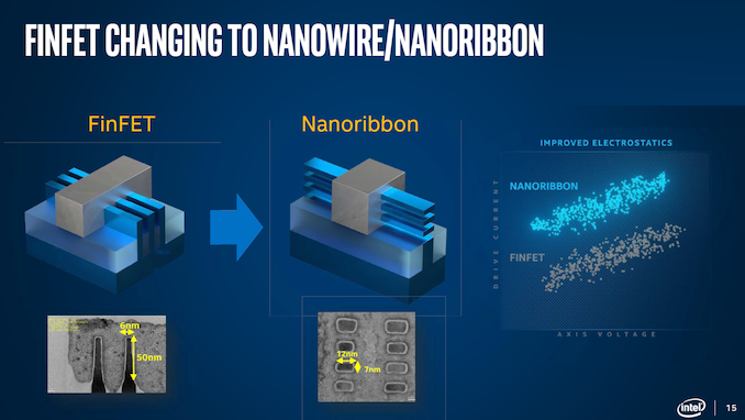
This year, at the international VLSI conference, Intel’s CTO Mike Mayberry gave one of the plenary presentations, which this year was titled ‘The Future of Compute’. Within the presentation, a number of new manufacturing technologies were discussed, including going beyond FinFET to Gate-All-Around structures, or even to 2D Nano-sheet structures, before eventually potentially leaving CMOS altogether. In the Q&A at the end of the presentation, Dr. Mayberry stated that he expects nanowire transistors to be in high volume production within five years, putting a very distinctive mark in the sand for Intel and others to reach.
Finned transistors, as introduced by Intel at ‘22nm’ and everyone else at ‘16nm’, were a way of scaling the drive current beyond a planar transistor, a key metric in enabling both density and high performance logic. Intel is currently on its multi-generation FinFET design, with each generation increasing the height of the fins in order to help boost the key metrics. As with planar transistors however, there is a limit somewhere between a natural limit and a manufacturing limit where another shift in the transistor design is needed. In this case, Gate-All-Around designs, which have been in research and development for over a decade or more, or needed.
From Samsung
There are a number of different names for Gate-All-Around (GAA) designs. The GAA implementation essentially looks like a hovering transistor fin, which can be either really small (nanowire) or wider (nanosheet), with multiple stacked wires or sheets increasing the effective width of the transistor when it comes to drive current metrics. GAA, for most foundry businesses, has expected to intersect with the ‘3nm’ node, which should offer similar density to Intel’s ‘5nm node’.
One of the key benefits of these GAA transistors is that the transistor can be specifically tailored to the operational requirements. A typical transistor with a FinFET might require a cell height of 6-7 discrete fins, and thus the drive current is a function of fin count. With a GAA type design, not only implementing stacking but sheet width as well, the drive current is now a continuous spectrum, which should allow for space savings and power savings at a silicon level. Whereas FinFETs only have one power/frequency design point within a process node design for a given fin count, GAA allows a continuous scale in transistor design.

From Samsung
Samsung has already announced its intention to deliver GAA transistors into its manufacturing process at the stage where it hits a ‘3nm’ process node. In May 2019, the company put out a press release as part of its Foundry Forum that the first beta version of the PDK, v0.1, was ready for its foundry customers to start experimenting. At the time, Samsung expected the first trial runs of its 3GAE process to tapeout in 2020, with risk production in late 2020, with volume manufacturing in late 2021.
During the 2020 VLSI Symposia on Technology and Circuits, Intel’s CTO and GM of Technology Development, Dr. Mike Mayberry, gave one of the plenary talks on ‘The Future of Compute’. In the detailed presentation, Dr. Mayberry covered a good deal about how compute is permeating at every level, from device to edge to datacenter, and how the demand for low-latency and high performance are key elements driving that change. With that comes a number of design options and opportunities, but also complexity, cost, and compute barriers. One of the requirements to drive paradigm shifts is change at the manufacturing level, going beyond FinFET technology, when we expect every major foundry on the leading edge to start introducing GAA technology. Dr. Mayberry covered domain specific architectures, memory and power management, security, system complexity, directed self-assembly, 3D transistor stacking, heterogeneous integration and packaging, as well as going beyond standard computing paradigms or even CMOS as ways to continue to push both the limits of compute but also the ubiquity of compute.
There were a few slides that might be worth covering in a future article, along with a few of the Q&A parts, however it was this question where Dr. Mayberry said a point worth reporting.
Q: Can you give us the timeline for the introduction of nanoribbon/nanowire process technology into high volume production?
A: This is not a roadmap talk, so I'll be vague and say within in the next five years.
Here’s our video cut from the discussion:
It’s hard not to give hints about roadmaps and timelines when stating when a given technology is going to be ready, so despite Dr. Mayberry stating he would be vague, it does kind of help us narrow down some of Intel’s plans.
It is worth noting that neither the question nor did Dr. Mayberry say this was a predicted timeline for Intel’s implementation, and he could have been speaking more about Intel’s competitors. However in these sorts of talks, discussing the competition is often frowned upon a lot internally, so this is why we’re under the impression that this was focused more on Intel’s ability to produce GAA than anyone else.
Given what we know about Intel’s timeline, we have this slide from Intel, as presented in September 2019 at the SPIE conference:
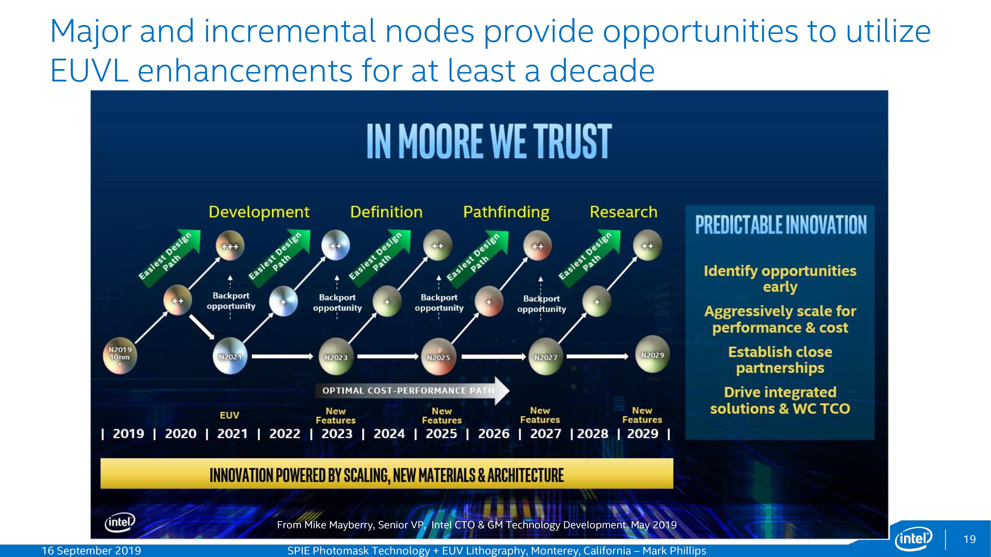
For 2021, Intel is preparing 10+++ as well as a new process node (7nm), and we know this to be the case given that Intel has a contract with the Aurora supercomputer for Argonne, which is due to have Intel’s new Ponte Vecchio HPC accelerator inside, which is partly built on 7nm. That system has to be delivered in 2021, or at least Intel has to hit a number of minimum milestones for that system in 2021, so we might see the first inklings of 7nm at that time. The slide above also says 7nm on EUV.
Assuming all goes to plan, we have 2022 with 7+, then 2023 with 7++ and another new process node, believed to be 5nm. This is expected to be the inflection point with TSMC’s 3nm in terms of density, which could suggest that this is where GAA technology is likely to be.
Going beyond that, 2024 is 5+, then 2025 is 5++ and 3nm. If I were a betting man, and I predicted that Intel’s timeline over the course of five years might slip the best part of 6-12 months, then 2025 might still be in the 5nm / 5+ era. So with Dr. Mayberry saying within 5 years for high volume, the smart money would be GAA coming at 5nm, in 2023-2024.

This was one of the final slides of the presentation, showcasing where Intel is looking over the next 15 years. Quantum is so far outside the scope of anything else Intel is doing that Dr. Mayberry said that it is so far away at this point. However, Intel is making steps towards Deep Learning, Graph Analytics, and Neuromorophic compute.
Related Reading:
- Samsung Announces 3nm GAA MBCFET PDK, Version 0.1
- Intel’s Manufacturing Roadmap from 2019 to 2029: Back Porting, 7nm, 5nm, 3nm, 2nm, and 1.4 nm
- Ten Year Anniversary of Core 2 Duo and Conroe: Moore’s Law is Dead, Long Live Moore’s Law
- Samsung Starts Mass Production at V1: A Dedicated EUV Fab for 7nm, 6nm, 5nm, 4nm, 3nm Nodes
- Analyzing Intel’s Discrete Xe-HPC Graphics Disclosure: Ponte Vecchio, Rambo Cache, and Gelato
- Intel’s 2021 Exascale Vision in Aurora: Two Sapphire Rapids CPUs with Six Ponte Vecchio GPUs
- Intel’s Xe for HPC: Ponte Vecchio with Chiplets, EMIB, and Foveros on 7nm, Coming 2021


13 Comments
View All Comments
bhd2 - Monday, June 22, 2020 - link
Note the TARDIS in the background in his office! Another Dr. Who fan!PeterMorgan573 - Monday, June 22, 2020 - link
Although your final comments emphasize that Intel is mostly not in the business of QC, the increasingly analog nature of the low-level hardware that you mention earlier, "With a GAA type design, not only implementing stacking but sheet width as well, the drive current is now a continuous spectrum", pushes us also towards designs where the probability of binary errors has to be more accommodated. To widen the perspective that I intend by this comment, QC can be taken to be about engineering the noise in a system as a way to engineer faster implementations of specific algorithms. As the effects of noise become more significant in smaller scale circuits, a step to engineering noise to use it positively for specific algorithms instead of engineering noise to make it have no effect on algorithms may be a transition that Intel (and other manufacturers with very extensive understanding of materials and process technology) will be able to push through more smoothly than might be expected as of now. Many factors may intervene, of course, and this obviously comes from a very specific perspective on QM and QC.Santoval - Sunday, June 28, 2020 - link
"the increasingly analog nature of the low-level hardware that you mention earlier.."Only the current supply of a GAA-FET transistor becomes quasi-analogue (as opposed to *discrete* rather than digital or binary), however that would not affect the computing paradigm by somehow making it less digital and more analogue. Why/how would/could it?
The "continuous" rather than discrete drive current will simply give semiconductor engineers better flexibility in extracting higher energy efficiency from their design, as is mentioned in the article, which is important. I also don't see any connection to quantum computing, which is another matter entirely.
azfacea - Monday, June 22, 2020 - link
intel's biggest problem is the "sales dept lead" market control mentality that leads to saying no to every expansion or capacity expansion opportunity. they are the opposite of elon musk. They could have taken dozens of different process node technologies to high volume production by now, instead they do only two in 5 years. they could've built more fabs and drive down their costs with better amortization but instead they hope to control supply and jack up prices. I dont think they have learned. they have no vision, no desire to solve new problems or even old ones like dram. complete opposite of Elon, he wants to solve every problem he runs into. Honestly Tesla is more likely to get into something new like MRAM than Intel at this point. Intel is sitting there hoping to find the right person(s), hire them, get back to leading edge and everything can stabilize.thats not how it works. the Newtonian universe does not exist. you either expand or you contract.
JayNor - Monday, June 22, 2020 - link
"Intel Demonstrates STT-MRAM for L4 Cache"https://www.tomshardware.com/news/intel-demonstrat...
brantron - Monday, June 22, 2020 - link
Wut. Intel has expanded capacity, and changed manufacturing processes at the same pace as AMD and Nvidia.It would be nice if the conspiracy theories people come up with were even remotely plausible. TIL Intel "hopes to control supply." Why, AMD would double wafer orders in the face of overstock reports!
TheJian - Tuesday, June 30, 2020 - link
If that was the case they wouldn't have hired TSMC and Samsung to produce chips for them at 14nm never mind the 10nm issues for years. They had an empty fab down the road from me for years. Apple almost went 1/2 on it ages ago.They blew 4B+ a year for 4+ years on mobile rather than spending that 15-20B on FABS. That is why 10nm is 3-4yrs late. It is why they are no longer in the lead. PERIOD. They also refused for ages to make OTHER products. They could have easily won mobile if they had made a deal to buy out NV, and make socs/gpus that would have filled even more fabs and cemented their lead for decades. They could have easily made a cpu that played windows or arm. Not saying they can't get back (good roadmap if they can hit it), but they are not the leader of fabs today. PERF etc don't lie. TSMC has they beat for now (samsung maybe too). I see a time I may buy Intel again (stock).
AMD DID double wafers, as they bought ALL of the 15% of capacity apple was taking from 7nm. That 15% happens to double AMD's old 15%, so now roughly 30% of TSMC 7nm going AMD in some shape or form? This site itself said they bought it ALL (among others saying the same). If this is true, AMD is #1 at TSMC 7nm now. I'm guessing they're piling up launch chips for Q4 right now with those wafers.
What overstock reports? Intel can't fill 10% of their customer's orders (dell, hp, lenovo, etc whining), so I think it's a safe bet AMD wants some of those orders. How many chips does 10% of Intel's customers equal? 280mil chips sold yearly, gpus on top, consoles, custom apu. AMD has a lot of stuff to double their take. Going from 15% to 30% is doubling wafers, so should be near double chips unless you massively grow your dies. I don't hear that happening as next launch is 8c apu with a gpu far short of where I'd put it, so not a large die here. Next gpu isn't until 2021 IMHO but they say 2020. In AMD's opinion that could be Xbox/ps5. I don't count it as RDNA2 until it's in a PC desktop or laptop, not a console, but obviously they are both launching around Q4/Q1 so a large amount of silicon will be going to both for launches (think 5-10mil each in the next 6 months, so gpu later IMHO).
Either way, consoles will be a large die going for 4k (ROFL, whatever), RTX stuff, last size of original xbox1/ps4 were ~360mm^2 IIRC. I think even Xbox X is supposedly 400mm^2 or so roughly if rumors are true. So again, quite a large piece of silicon going out for millions of xbox/ps5 consoles. That size of die adds up quick when you are used to making 100-250mm^2 for most of your stuff. Never mind SERVER dies that use that or far more in what is coming. What will 128c take? Can they do a 7nm 128c (7nm+ EUV rumor for zen3 4000 series) with decent speeds/watts? We'll see, but those would be large I'd guess no matter what way they go :) No worries, silicon shortages coming probably for the next year as companies go back to work and buy silicon regardless of people. They can't quit the server, AI, cloud, car wars. Enterprise has no choice, innovate, or someone else takes all these over first and you're left with crumbs.
Checking a Epyc Rome die, 416 (cpus)+125 (IOD)+some other stuff, 1008mm^2 total silicon if I'm reading the pic right...LOL. Either way, again, many ways to spend double AMD silicon if you have BETTER products. I'd guess at some point Intel won't have shortages and instead will have overstock reports :) I see emptying shelves for new products (NV been doing it for a while, amd too probably). Intel is probably having issues dumping stuff that sucks in many things vs. AMD currently, but fortunately it would seem most of AMD's new silicon went to consoles (another dumb move, go after RICH, then poor consoles for $10-20 a chip). They just don't seem to know how to make HIGH MARGIN stuff FIRST. They always go no margin junk apu/console, then the money makers when it's too late, NV/Intel already collected. Looks like we'll do it again. AMD will have 1B NET INCOME per Q when they quit wasting silicon on consoles before FLAGSHIP CPU/GPU/SERVER. Aim high, go low only when forced. I wouldn't make a single piece of silicon for poor people (cpus under $200, gpu same) until servers were no longer selling and some were stuck on the shelf. ONLY then, do you make a lower margin product as the little guy in this game.
Also note, simply doubling wafers doesn't magically have 2x wafers pop out tomorrow. You have to rejig designs for a (potentially new process for product X) new process, or product that IS a new design itself, etc etc. IT is months before you tool up for new products before you see it on a shelf. Apple doesn't cancel 7nm 1 day and pump out 5nm 24hrs later. That takes time, then time for AMD or whoever takes their place to tape out more chips on said older process (7nm in this case for AMD) Either way, CUSTOMERS WIN here IMHO. More stuff floating around, we get better chips, at better cost and they have no way to avoid the war really. TEch is going to be great for buyers for the next 3-5yrs. Massively explosions coming in perf/watts/features etc now coming into view. We just saw 830mm^2 max, then shortly after 1600mm^2+, now talking 3500mm^2+ dies. We have everyone talking packaging tech, etc. Massive power incoming from MANY directions of tech in silicon. Lots of fun coming, upgrade your life so you can afford more toys people :)
Off work? Take some training courses to raise your value while off, go back stronger and worth MORE $$$. Or just wait until the toys you want come down a year later. Wait or make more bank. :)
soresu - Monday, June 22, 2020 - link
Ugh... typical Intel contrary naming scheme.What happened to their "magneto electric spin orbit transistors are the next big thing...." speech last year?
I guess not much is the answer.
MBravo - Monday, June 22, 2020 - link
Does anybody know where can I see entire talk? Or is everything behind a paywall?edzieba - Monday, June 22, 2020 - link
Intel are already using variable numbers of fins/transistor to tune transistor operation on the same die (e.g. trading off current capacity vs. leakage), so this gives them more flexibility in varying gate width directly rather than in discrete steps.