Intel to use Nanowire/Nanoribbon Transistors in Volume ‘in Five Years’
by Dr. Ian Cutress on June 22, 2020 8:00 AM EST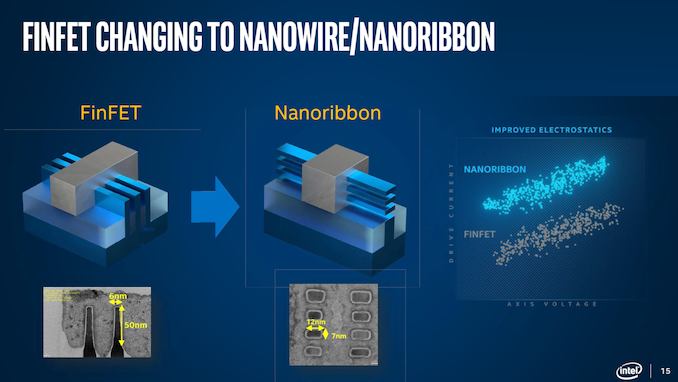
This year, at the international VLSI conference, Intel’s CTO Mike Mayberry gave one of the plenary presentations, which this year was titled ‘The Future of Compute’. Within the presentation, a number of new manufacturing technologies were discussed, including going beyond FinFET to Gate-All-Around structures, or even to 2D Nano-sheet structures, before eventually potentially leaving CMOS altogether. In the Q&A at the end of the presentation, Dr. Mayberry stated that he expects nanowire transistors to be in high volume production within five years, putting a very distinctive mark in the sand for Intel and others to reach.
Finned transistors, as introduced by Intel at ‘22nm’ and everyone else at ‘16nm’, were a way of scaling the drive current beyond a planar transistor, a key metric in enabling both density and high performance logic. Intel is currently on its multi-generation FinFET design, with each generation increasing the height of the fins in order to help boost the key metrics. As with planar transistors however, there is a limit somewhere between a natural limit and a manufacturing limit where another shift in the transistor design is needed. In this case, Gate-All-Around designs, which have been in research and development for over a decade or more, or needed.
From Samsung
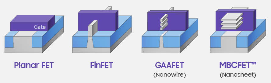
There are a number of different names for Gate-All-Around (GAA) designs. The GAA implementation essentially looks like a hovering transistor fin, which can be either really small (nanowire) or wider (nanosheet), with multiple stacked wires or sheets increasing the effective width of the transistor when it comes to drive current metrics. GAA, for most foundry businesses, has expected to intersect with the ‘3nm’ node, which should offer similar density to Intel’s ‘5nm node’.
One of the key benefits of these GAA transistors is that the transistor can be specifically tailored to the operational requirements. A typical transistor with a FinFET might require a cell height of 6-7 discrete fins, and thus the drive current is a function of fin count. With a GAA type design, not only implementing stacking but sheet width as well, the drive current is now a continuous spectrum, which should allow for space savings and power savings at a silicon level. Whereas FinFETs only have one power/frequency design point within a process node design for a given fin count, GAA allows a continuous scale in transistor design.

From Samsung
Samsung has already announced its intention to deliver GAA transistors into its manufacturing process at the stage where it hits a ‘3nm’ process node. In May 2019, the company put out a press release as part of its Foundry Forum that the first beta version of the PDK, v0.1, was ready for its foundry customers to start experimenting. At the time, Samsung expected the first trial runs of its 3GAE process to tapeout in 2020, with risk production in late 2020, with volume manufacturing in late 2021.
During the 2020 VLSI Symposia on Technology and Circuits, Intel’s CTO and GM of Technology Development, Dr. Mike Mayberry, gave one of the plenary talks on ‘The Future of Compute’. In the detailed presentation, Dr. Mayberry covered a good deal about how compute is permeating at every level, from device to edge to datacenter, and how the demand for low-latency and high performance are key elements driving that change. With that comes a number of design options and opportunities, but also complexity, cost, and compute barriers. One of the requirements to drive paradigm shifts is change at the manufacturing level, going beyond FinFET technology, when we expect every major foundry on the leading edge to start introducing GAA technology. Dr. Mayberry covered domain specific architectures, memory and power management, security, system complexity, directed self-assembly, 3D transistor stacking, heterogeneous integration and packaging, as well as going beyond standard computing paradigms or even CMOS as ways to continue to push both the limits of compute but also the ubiquity of compute.
There were a few slides that might be worth covering in a future article, along with a few of the Q&A parts, however it was this question where Dr. Mayberry said a point worth reporting.
Q: Can you give us the timeline for the introduction of nanoribbon/nanowire process technology into high volume production?
A: This is not a roadmap talk, so I'll be vague and say within in the next five years.
Here’s our video cut from the discussion:
It’s hard not to give hints about roadmaps and timelines when stating when a given technology is going to be ready, so despite Dr. Mayberry stating he would be vague, it does kind of help us narrow down some of Intel’s plans.
It is worth noting that neither the question nor did Dr. Mayberry say this was a predicted timeline for Intel’s implementation, and he could have been speaking more about Intel’s competitors. However in these sorts of talks, discussing the competition is often frowned upon a lot internally, so this is why we’re under the impression that this was focused more on Intel’s ability to produce GAA than anyone else.
Given what we know about Intel’s timeline, we have this slide from Intel, as presented in September 2019 at the SPIE conference:
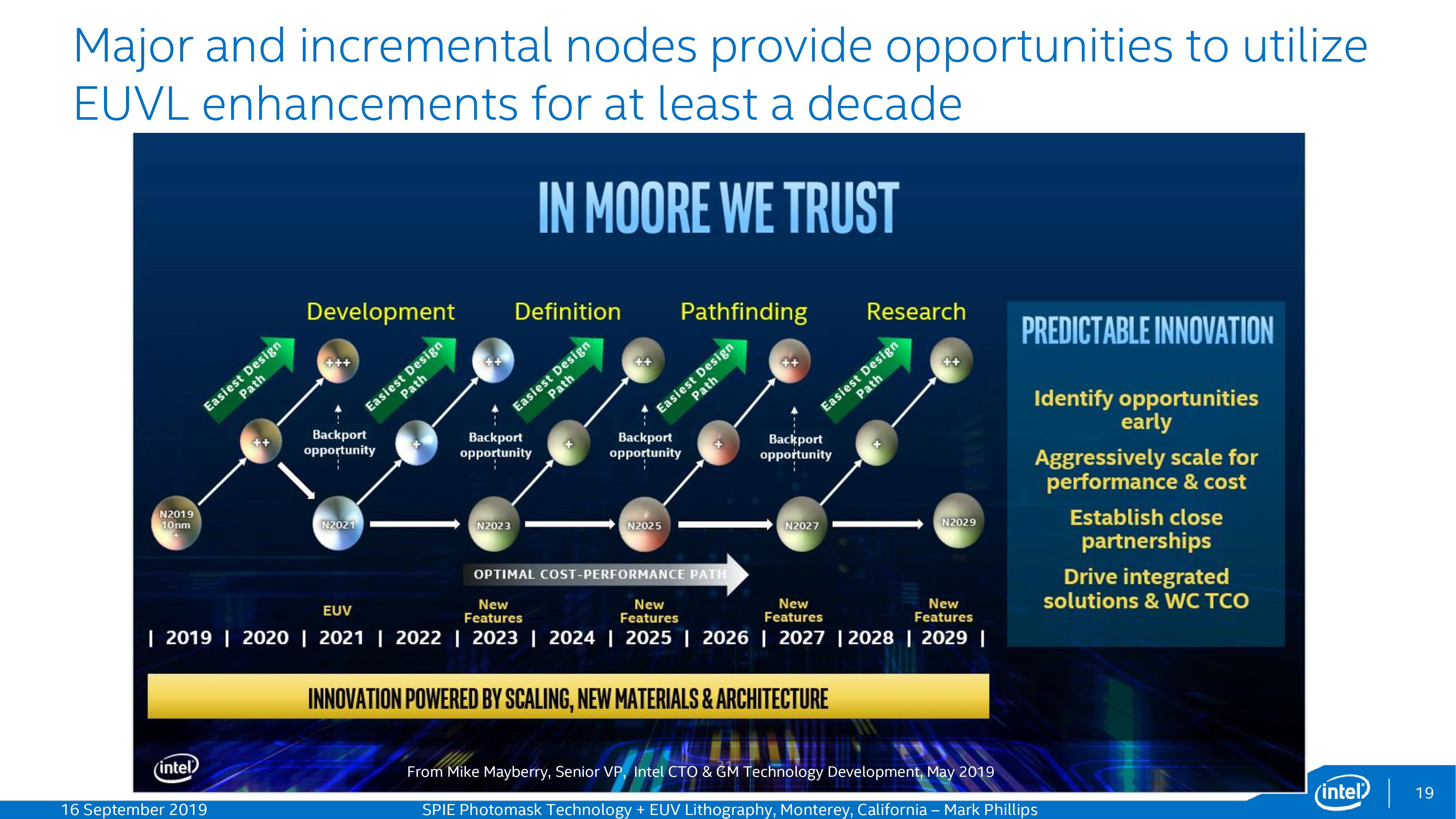
For 2021, Intel is preparing 10+++ as well as a new process node (7nm), and we know this to be the case given that Intel has a contract with the Aurora supercomputer for Argonne, which is due to have Intel’s new Ponte Vecchio HPC accelerator inside, which is partly built on 7nm. That system has to be delivered in 2021, or at least Intel has to hit a number of minimum milestones for that system in 2021, so we might see the first inklings of 7nm at that time. The slide above also says 7nm on EUV.
Assuming all goes to plan, we have 2022 with 7+, then 2023 with 7++ and another new process node, believed to be 5nm. This is expected to be the inflection point with TSMC’s 3nm in terms of density, which could suggest that this is where GAA technology is likely to be.
Going beyond that, 2024 is 5+, then 2025 is 5++ and 3nm. If I were a betting man, and I predicted that Intel’s timeline over the course of five years might slip the best part of 6-12 months, then 2025 might still be in the 5nm / 5+ era. So with Dr. Mayberry saying within 5 years for high volume, the smart money would be GAA coming at 5nm, in 2023-2024.

This was one of the final slides of the presentation, showcasing where Intel is looking over the next 15 years. Quantum is so far outside the scope of anything else Intel is doing that Dr. Mayberry said that it is so far away at this point. However, Intel is making steps towards Deep Learning, Graph Analytics, and Neuromorophic compute.
Related Reading:
- Samsung Announces 3nm GAA MBCFET PDK, Version 0.1
- Intel’s Manufacturing Roadmap from 2019 to 2029: Back Porting, 7nm, 5nm, 3nm, 2nm, and 1.4 nm
- Ten Year Anniversary of Core 2 Duo and Conroe: Moore’s Law is Dead, Long Live Moore’s Law
- Samsung Starts Mass Production at V1: A Dedicated EUV Fab for 7nm, 6nm, 5nm, 4nm, 3nm Nodes
- Analyzing Intel’s Discrete Xe-HPC Graphics Disclosure: Ponte Vecchio, Rambo Cache, and Gelato
- Intel’s 2021 Exascale Vision in Aurora: Two Sapphire Rapids CPUs with Six Ponte Vecchio GPUs
- Intel’s Xe for HPC: Ponte Vecchio with Chiplets, EMIB, and Foveros on 7nm, Coming 2021


13 Comments
View All Comments
name99 - Monday, June 22, 2020 - link
"Dr. Mayberry stated that he expects nanowire transistors to be in high volume production within five years"Sure, we all expect this.
The question is whether Dr. Mayberry, or anyone else, expects Intel to be manufacturing any of them!
Adonisds - Tuesday, June 23, 2020 - link
When Intel moved to finfet clocks got substantially reduced compared to sandy bridge. What can we probably expect of the overclocking potential of gaafet?sonicmerlin - Saturday, June 27, 2020 - link
But even with shrinking transistors, CPU speeds barely improve with each generation.