New #1 Supercomputer: Fugaku in Japan, with A64FX, take Arm to the Top with 415 PetaFLOPs
by Dr. Ian Cutress on June 22, 2020 11:00 AM EST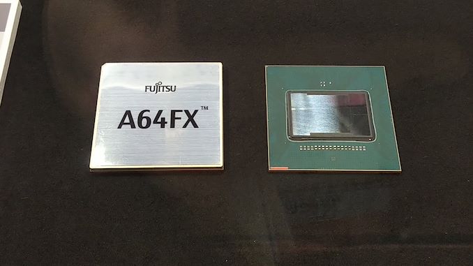
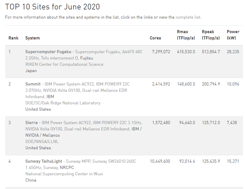
High performance computing is now at a point in its existence where to be the number one, you need very powerful, very efficient hardware, lots of it, and lots of capability to deploy it. Deploying a single rack of servers to total a couple of thousand cores isn’t going to cut it. The former #1 supercomputer, Summit, is built from 22-core IBM Power9 CPUs paired with NVIDIA GV100 accelerators, totaling 2.4 million cores and consuming 10 MegaWatts of power. The new Fugaku supercomputer, built at Riken in partnership with Fujitsu, takes the top spot on the June 2020 #1 list, with 7.3 million cores and consuming 28 MegaWatts of power.
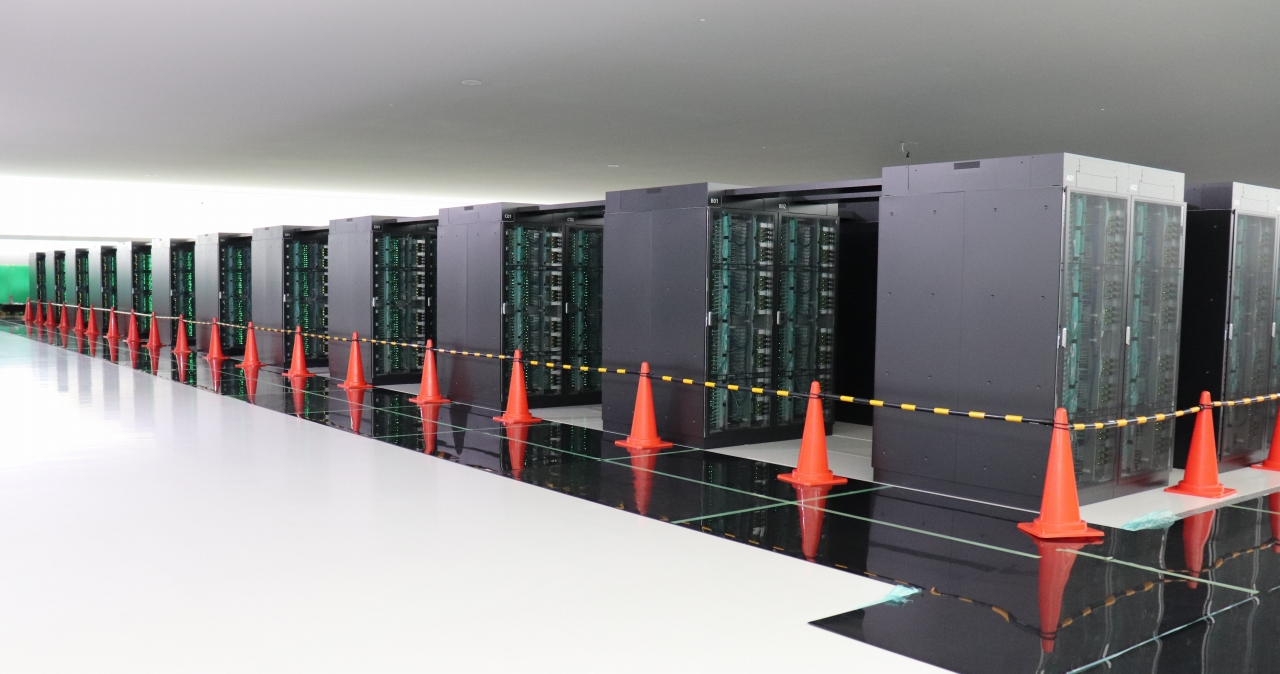
The new Fugaku supercomputer is bigger than Summit in practically every way. It has 3.05x cores, it has 2.8x the score in the official LINPACK tests, and consumes 2.8x the power. It also marks the first time that an Arm based system sits at number one on the top 500 list.
Due to the onset of the Coronavirus pandemic, Riken accelerated the deployment of Fugaku in recent months. On May 13th, Riken announced that more than 400 racks, each featuring multiple 48-core A64FX cards per server, were deployed. This was a process that had started back in December, but they were so keen on getting the supercomputer up and running to assist with the R&D as soon as possible – the server racks didn’t have their official front panels when they started working. There are still additional resources to add, with full operation scheduled to begin in Riken’s Fiscal 2021, suggesting that Fugaku’s compute values on the top 100 list are set to rise even higher.
Alongside being #1 in the TOP500, Fugaku enters the Green500 List at #9, just behind Summit, and below the Fugaku Prototype installation which sits at #4.

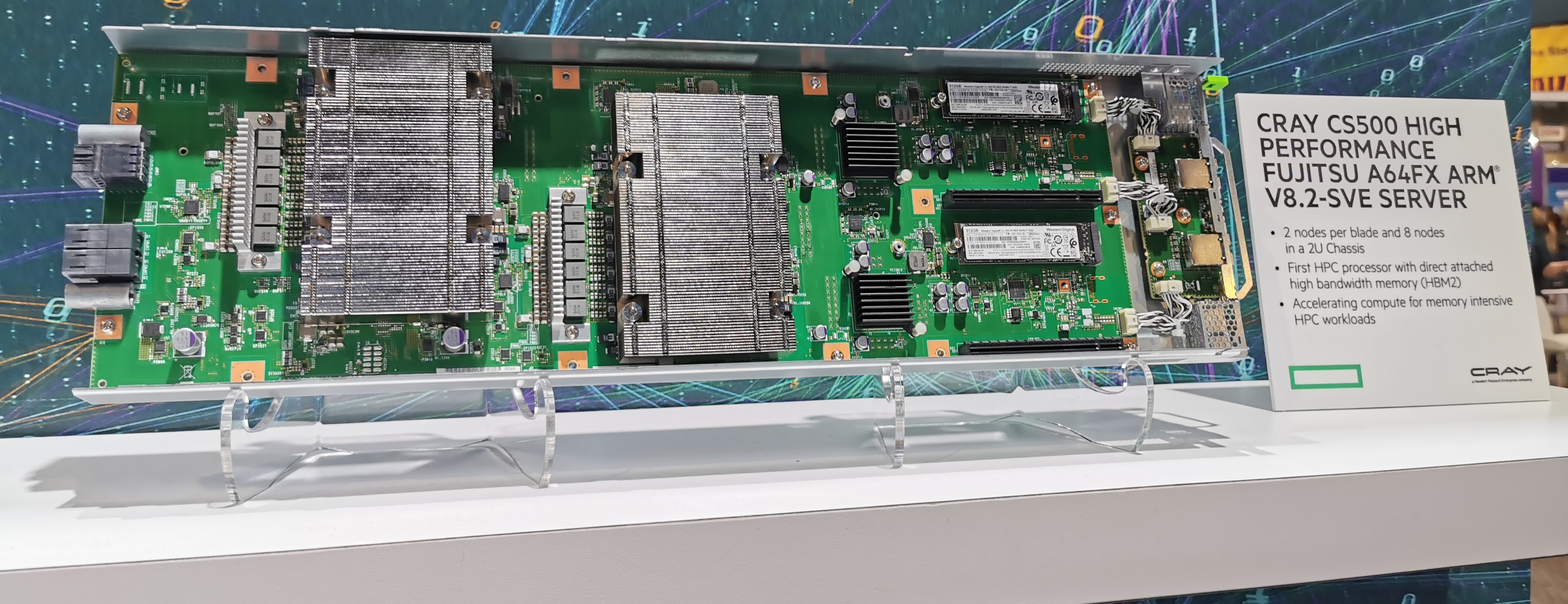
At the heart of Fugaku is the A64FX, a custom Arm v8-A CPU-based chip optimised for compute. The total configuration uses 158,976 of these 48+4-core cards, running at 2.2 GHz peak performance (48 cores for compute, 4 for assistance). This allows for some substantial Rpeak numbers, such as 537 PetaFLOPs of FP64, the usual TOP500 metric. But A64FX also supports quantized models with lower precision, which is where we get into some fun numbers for Fugaku:
- FP64: 0.54 ExaFLOPs
- FP32: 1.07 ExaOPs
- FP16: 2.15 ExaOPs
- INT8: 4.30 ExaOPs
Due to the design of the A64FX, it also allows for a total memory bandwith of 163 PetaBytes per second.
To date, the A64FX compute card is the only implementation of Arm’s v8.2-A Scalable Vector Extensions (SVE). The goal of SVE is to allow Arm’s customers to build hardware with vector units ranging from 128-bit to 2048-bit, such that any software that is built to run on SVE will automatically scale regardless of the SVE execution unit size. A64FX uses two 512-bit wide pipes per core, with 48 compute cores per chip, and also adds in four 8 GiB HBM2 links per chip in order to feed the units for 1 TiB/s of total bandwidth into the chip.
As listed above, the unit supports INT8 through FP64, and the chip has an on-board custom Tofu interconnect, supporting up to 560 Gbps of interconnect to other A64FX modules. The chip is built on TSMC’s N7 process, and comes in at 8.79 billion transistors. 90% execution efficiency is claimed for DGEMM type workloads, and additional mechanisms such as combined gather and unaligned SIMD loading are used to help keep throughput high. There is also additional tuning that can be done at the power level for optimization, and extensive internal RAS (over 128k error checkers in silicon) to ensure accuracy.

Details on the A64FX chip were disclosed at Hot Chips in 2018, and we saw wafers and chips at Supercomputing in 2019. This chip is expected to be the first in a series of chips from Fujitsu along a similar HPC theme.

Work done on Fugaku to date includes simulations about Japan’s COVID-19 track and tracing app. According to Professor Satoshi Matsuoka, predictions calculated by Fugaku suggested a 60% distribution on the app development in order to be successful. Droplet simulations have also been performed on virus activity. Deployment of A64FX is set to go beyond Riken, with Sandia Labs to also have an A64FX system based in the US.
Source: TOP500
Related Reading
- A Success on Arm for HPC: We Found a Fujitsu A64FX Wafer
- Hot Chips 2018: Fujitsu's A64FX Arm Core Live Blog


46 Comments
View All Comments
thetrashcanisfull - Monday, June 22, 2020 - link
But SVE *does* have inter-lane (shuffle/permute) instructions; how Fujitsu has implemented those instructions (pipelined or in microcode) remains an open question, but SVE does support them.name99 - Monday, June 22, 2020 - link
Of course SVE has inter-lane operations! Where do people pick up this nonsense?Obviously it has the usual reductions, but it also has a variety of standardized shuffles that generalize to length agnostic (eg interleaves) AND the TBL (table lookup) instruction which is the one (and only, as far as I know) none-length-agnostic instruction -- but it is there if you need generic permutes and are willing to code to that particular machine and nothing else.
mode_13h - Tuesday, June 23, 2020 - link
I said "if", based on the assumption that they were trying to do pure SIMD with it, in order to try and compete with GPUs. It was literally the first word. No reason you can't see it there.I think GPUs don't support inter-lane operations because they could involve rather a lot of silicon, for large vectors. Not simple interleaving, but things like horizontal arithmetic and arbitrary shuffles.
Dolda2000 - Monday, June 22, 2020 - link
You could certainly argue that the SIMD units are GPU-like, but yeah, it's a homogeneous architecture. It's really, really nice that they're even attempting that in the current year, I really hope it works out well for them. I'm also curious what the practical differences really are vs. Xeon Phi (which on paper is quite similar with 2x512-bit FMAs per core) and why they expect this to work out better. Better intetconnect?nft76 - Monday, June 22, 2020 - link
The nodes are thin by modern standards (only 3.4 TFLOPS and 32 GB memory), so the interconnect really has to be good. A large simulation will be spread over a huge number of nodes and there will be a lot of MPI communication.mode_13h - Monday, June 22, 2020 - link
With regard to Xeon Phi: exactly. It seems to me they're basically counting on the benefits of a superior ISA, but it's still not going to beat GPUs at their own game.thetrashcanisfull - Monday, June 22, 2020 - link
I think the interconnect, as well as the broader system topology, is a big part of it. I also think that a more apt comparison might be to IBM's (now ancient) Blue Gene-Q processor: a many-core processor with integrated many-port networking, scaling to large node-counts with an unswitched (peer-to-peer) network topology, and (relatively) low per-node power usage.jeremyshaw - Monday, June 22, 2020 - link
Very cool. I find it interesting that Mervell isn't going the SVE route for their 4x128 FPU in the ThunderX3. There any specific reason for Fujitsu pursuing this? Or was this a flexible ISA extension given to largely (help?) move Fujitsu away from the dying (but open) SPARC ISA?SarahKerrigan - Monday, June 22, 2020 - link
SVE gives Fujitsu access to features they had in their proprietary HPC-ACE ISA before; going back to NEON would have been a massive regression. I also expect that ThunderX4 is going to be SVE-capable. Marvell has said SVE support is likely to be coming in the future.jeremyshaw - Monday, June 22, 2020 - link
I suppose that was the crux of my question: chicken or egg?