Intel Xe-HPC GPU Status Update: 4 Process Nodes Make 1 Accelerator
by Ryan Smith on August 13, 2020 12:00 PM EST- Posted in
- GPUs
- Intel
- Xe
- Ponte Vecchio
- Xe-HPC
- Intel Arch Day 2020

Continuing today’s GPU news from Intel’s Architecture Day presentation, on top of the Xe-LP architecture briefing and Xe-HPG reveal, the company has also offered a brief roadmap update for their flagship sever-level part, Xe-HPC.
Better known by its codename of Ponte Vecchio, much to do has been made about Xe-HPC. The most complex of the Xe parts planned, it is also the cornerstone of the Intel-powered Aurora supercomputer. Xe-HPC is pulling out all of the stops for performance, and to get there Intel is employing every trick in the book, including their new-generation advanced packaging technologies.
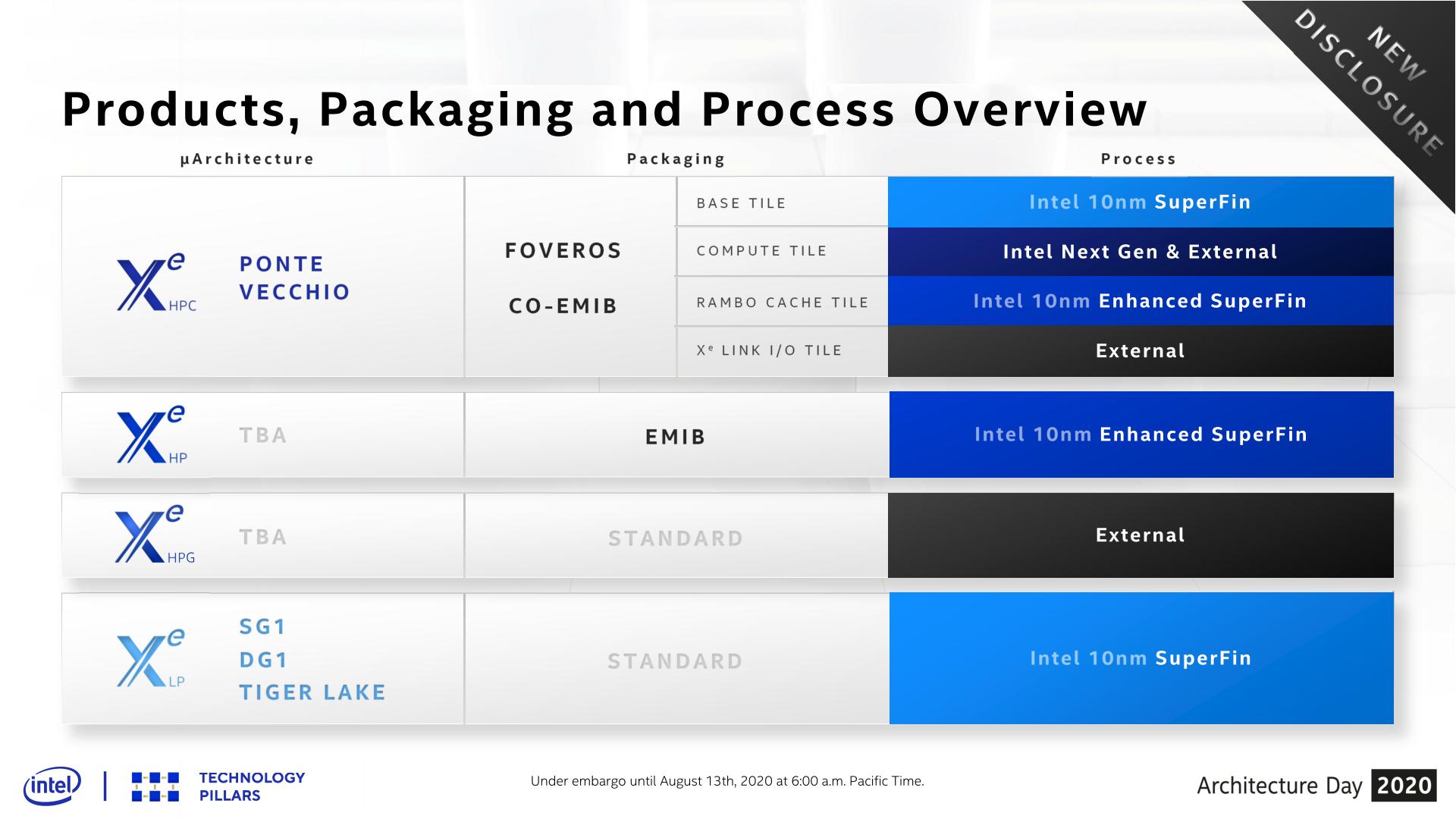
The big revelation here is that we finally have some more concrete insight into what manufacturing processes the various tiles will use. The base tile of the GPU will be on Intel’s new 10nm SuperFin process, and the Rambo Cache will be a generation newer still, using Intel’s future 10nm Enhanced SuperFin process. Meanwhile it’s now confirmed that the Xe Link I/O tile, which will be used as part of Intel’s fabric to link together multiple Xe-HPC GPUs, will be built by an external fab.
That leaves the matter of the compute tile, the most performance-critical of the GPU’s parts. With Intel’s 7nm process delayed by at least six months, the company has previously disclosed that they were going to take a “pragmatic” approach and potentially use third-party fabs. And as of their Architecture Day update, they still seem to be undecided about – or at least unwilling to disclose – just what they plan on doing. Instead, the compute die is labeled as “Intel Next Gen & External”.
It's an unusual disclosure, to say the least, as we'd otherwise expect the compute die to be made on a single process. But with no further commentary from Intel offered, make of that what you will. Perhaps they’re being straightforward, and they will actually use two very different process nodes for the compute die?


19 Comments
View All Comments
JayNor - Thursday, August 13, 2020 - link
Several GPU products coming in 2021, which is a bit of a surprise.Especially the hardware accelerated ray tracing so soon.
Krysto - Thursday, August 13, 2020 - link
Paper launches, most likely. It doesn't matter, as Intel's tactic of "getting people to wait for its GPUs" will not work. By the time these are on the market, people will be so blown away by Ampere/its refresh and RDNA 3 that they'll forget all about Intel's offerings, or find them boring.whatthe123 - Thursday, August 13, 2020 - link
Everyone is excited about Ampere.Nobody is excited about rdna3, including AMD who can't even confirm if they've locked down a node for it. RDNA2 on the series X is running around 2080 spec yet still around the same power envelope even though its on a superior node, with the series x eating up to 300w. Not exactly a good sign for RDNA3. AMD hit a homerun with their chiplet CPUs but are still just undercutting nvidia instead of competing in the GPU department.
intel, well, if its even vaguely performant that would be a huge surprise to everyone, so they've got a really low bar to work with.
FreckledTrout - Thursday, August 13, 2020 - link
I think you need to wait and see on RDNA2. You might be right. However I would not assume you can extrapolate from the custom ASIC from the XBOX to the dedicated GPU.Spunjji - Friday, August 14, 2020 - link
I don't think this is accurate at all. The OG RTX 2080 draws ~225W, and I haven't actually seen any solid specs for Series X power consumption yet - that 300W "estimate" appears to have originally come from Digital Foundry and was apparently based on the assumption that it would use RDNA. RDNA is already at approximate PPW parity with Turing, so seeing no improvement at all from RDNA 2 would be... unexpected.Personally I'd be surprised if the Series X pulls more than 250W total, given what we know about the thermal design and the clock speeds at which they're planning to run it; that would also be more in line with the claimed PPW improvements from RDNA to RDNA 2.
I'm not personally expecting RDNA 2 to take any performance crowns, but I am expecting it to compete *meaningfully* with Ampere at everything but the high-end.
PaulHoule - Thursday, August 13, 2020 - link
For a long time Intel has not even tried to have a public roadmap that makes sense. They have been so cagy at times it has been a threat to their business continuity.They might not hit their goals, but it is good to see that they have plans and goals. Also hearing that they are looking to foundries for 7nm means they have a plan B in case Intel 7nm ends up like Intel 10nm. That makes it much more likely we will have Intel around in 10 years.
damianrobertjones - Friday, August 14, 2020 - link
I wouldn't wish to mess with, 'Rambo Cache'.JayNor - Friday, August 14, 2020 - link
Intel didn't say their 7nm process is delayed by 6 months. They said their 7nm yields were low and their 7nm CPU schedules will be shifted by 6 months. Here is the quote from the q2 cc. Their 7nm cpus were already on the roadmap in 2022. Their Sapphire Rapids CPU in 2021 is 10nm."We are seeing an approximate six-month shift in our seven-nanometer-based CPU product timing relative to prior expectations. The primary driver is the yield of our seven-nanometer process"
JayNor - Friday, August 14, 2020 - link
Intel's announced DG1 is already available in devcloud.They've already demoed the ability to stitch together 4 HP tiles, so I'm going to go out on a limb and guess that they can stitch together four LP tiles to create the SG1.
They stated SG1 will be available in 2020.