A Broadwell Retrospective Review in 2020: Is eDRAM Still Worth It?
by Dr. Ian Cutress on November 2, 2020 11:00 AM ESTPower Consumption
The nature of reporting processor power consumption has become, in part, a dystopian nightmare. Historically the peak power consumption of a processor, as purchased, is given by its Thermal Design Power (TDP, or PL1). For many markets, such as embedded processors, that value of TDP still signifies the peak power consumption. For the processors we test at AnandTech, either desktop, notebook, or enterprise, this is not always the case.
Modern high performance processors implement a feature called Turbo. This allows, usually for a limited time, a processor to go beyond its rated frequency. Exactly how far the processor goes depends on a few factors, such as the Turbo Power Limit (PL2), whether the peak frequency is hard coded, the thermals, and the power delivery. Turbo can sometimes be very aggressive, allowing power values 2.5x above the rated TDP.
AMD and Intel have different definitions for TDP, but are broadly speaking applied the same. The difference comes to turbo modes, turbo limits, turbo budgets, and how the processors manage that power balance. These topics are 10000-12000 word articles in their own right, and we’ve got a few articles worth reading on the topic.
- Why Intel Processors Draw More Power Than Expected: TDP and Turbo Explained
- Talking TDP, Turbo and Overclocking: An Interview with Intel Fellow Guy Therien
- Reaching for Turbo: Aligning Perception with AMD’s Frequency Metrics
- Intel’s TDP Shenanigans Hurts Everyone
In simple terms, processor manufacturers only ever guarantee two values which are tied together - when all cores are running at base frequency, the processor should be running at or below the TDP rating. All turbo modes and power modes above that are not covered by warranty. Intel kind of screwed this up with the Tiger Lake launch in September 2020, by refusing to define a TDP rating for its new processors, instead going for a range. Obfuscation like this is a frustrating endeavor for press and end-users alike.
However, for our tests in this review, we measure the power consumption of the processor in a variety of different scenarios. These include full AVX2/AVX512 (delete as applicable) workflows, real-world image-model construction, and others as appropriate. These tests are done as comparative models. We also note the peak power recorded in any of our tests.
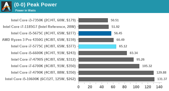
In peak power, the Core i7-5775C sticks to the 65 W value, whereas the Core i5 variant is below its TDP value. This is beyond the 22nm Core i7-4790S which is also a 65 W part.
In real-world tests, first up is our image-model construction workload, using our Agisoft Photoscan benchmark. This test has a number of different areas that involve single thread, multi-thread, or memory limited algorithms.
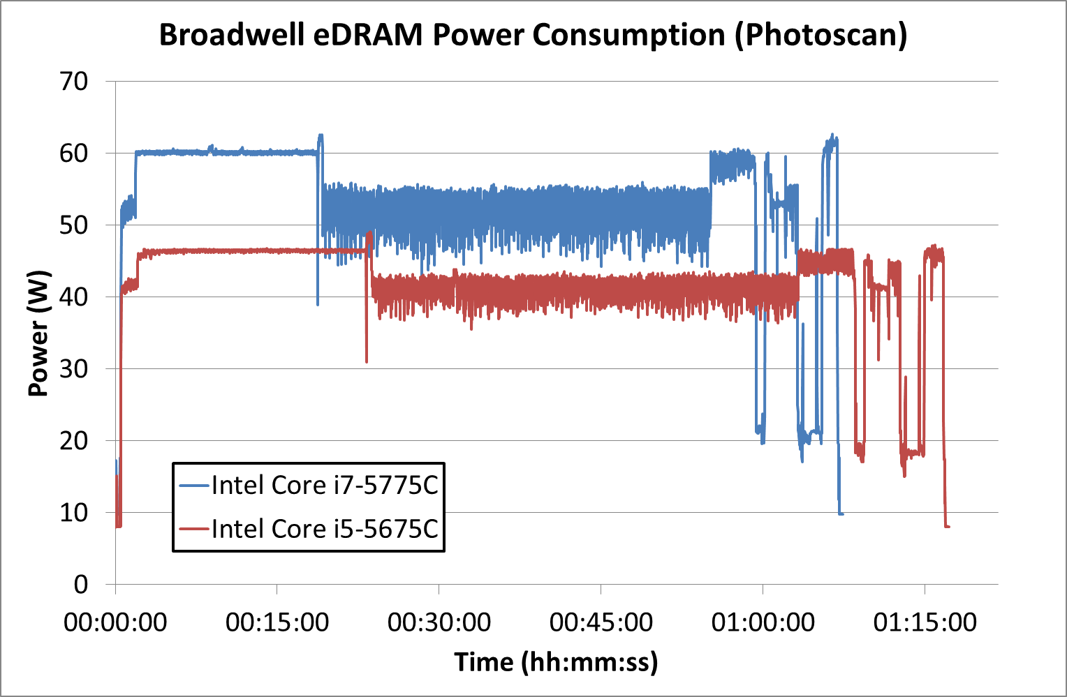
For Photoscan, the Core i7 spends its 'real world' time around 60 W, but does momentarily spike up above that 60 W mark. The Core i5 by comparison doesn't even touch 50 W.
The second test is from y-Cruncher, which is our AVX2/AVX512 workload. This also has some memory requirements, which can lead to periodic cycling with systems that have lower memory bandwidth per core options.
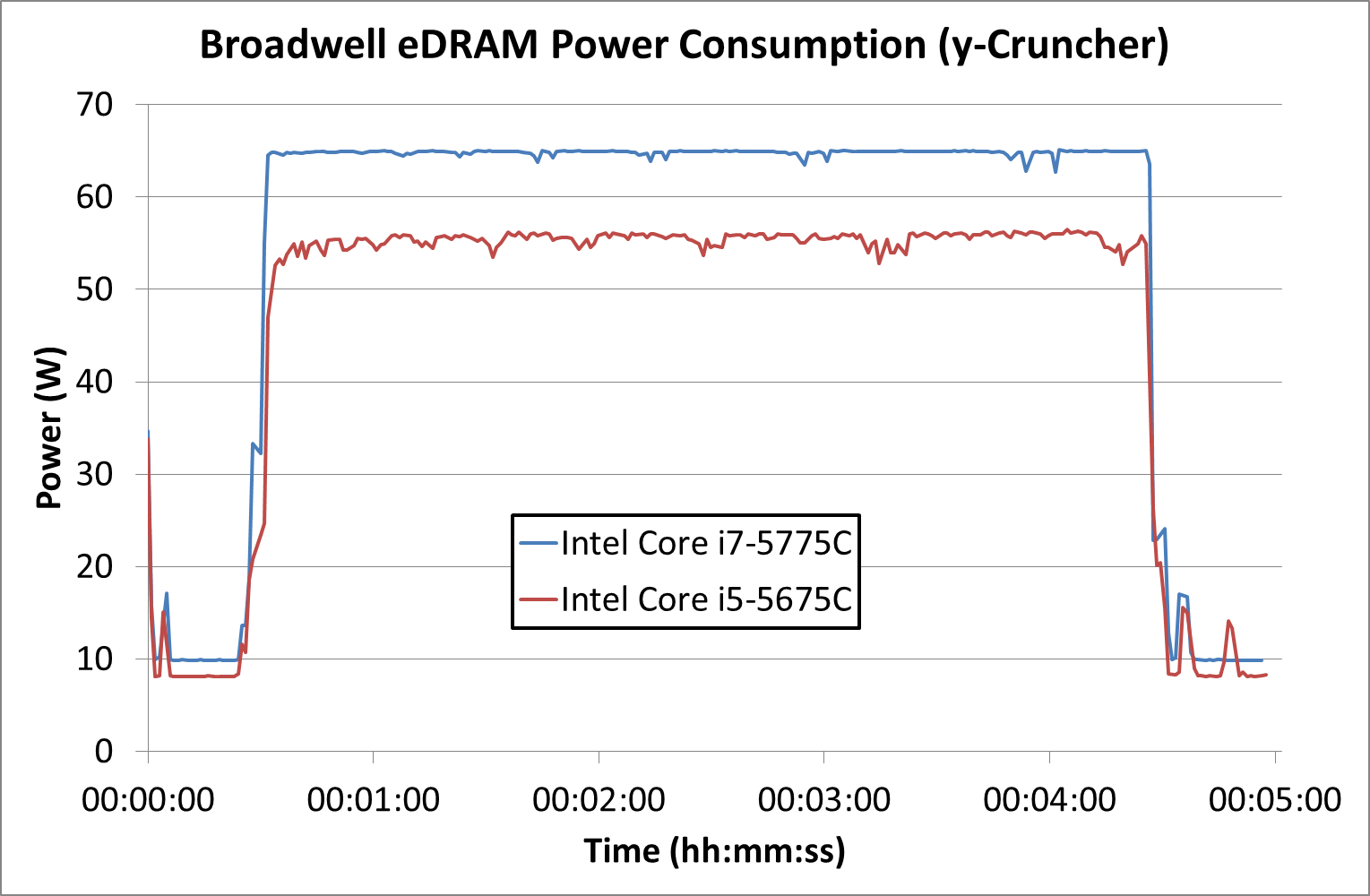
We're seeing some slight variation in power as the y-Cruncher algortihm moves out to DRAM movement over compute, however both processors seem to be hitting either their power limits or just a natural peak power consumption.


120 Comments
View All Comments
brucethemoose - Monday, November 2, 2020 - link
Is HBM2e access latency really lower than DDR4/5?I cant find any timing info or benchmarks, but my understanding is that its lower than GDDR6, which already has much higher latency than DDR4.
PeachNCream - Monday, November 2, 2020 - link
I'd like to say thanks for this review! I really love the look backwards at older hardware in relationship to modern systems. It really shows that in processor power terms that Broadwell/Haswell remain fairly relevant and the impact of eDRAM (or non-impact in various workloads) makes for really interesting reading.brucethemoose - Monday, November 2, 2020 - link
Another possibility: the "Radeon Cache" on an upcoming APU acts as a last level cache for the entire chip, just like Apple (and Qualcomm?) SoCs.Theres no extra packaging costs, no fancy 2nd chip, and it would save power.
Jorgp2 - Monday, November 2, 2020 - link
You do realize that Intel has had that about as long as they've had GPUs on their CPUs right?brucethemoose - Monday, November 2, 2020 - link
You mean the iGPUs share L3?Well, its wasn't a particularly large cache or powerful GPU until Broadwell came around.
Jorgp2 - Tuesday, November 3, 2020 - link
>Well, its wasn't a particularly large cache or powerful GPU until Broadwell came around.Larger than the caches on even AMDs largest GPUs until recently.
Hawaii had a 4MB cache, Vega had a 6MB I believe.
eastcoast_pete - Monday, November 2, 2020 - link
Thanks Ian, great article! Regarding a large, external L4 Cache: any guess on how speed and latency of eDRAM made in more modern silicon would compare with Broadwell's 22 nm one? Let's say if made in Intel's current 14 nm (++ etc)? And, if that'll speed it up enough to make it significantly better than current fast DDR4, would that be a way for Intel to put some "electronic nitrous" on its Tiger Lake and Rocket Lake chips? Because they do need something, or they'll get spanked badly by the new Ryzens.brucethemoose - Monday, November 2, 2020 - link
I'm guessing most of the latency comes from the travel between the chips, not from the speed of the eDRAM itself. So a shrink wouldnt help much, but EMIB might?There is talk of replacing on-chip SRAM in L3 cache with eDRAM, kind of like what IBM already does. So basically, its a size vs speed tradeoff, which is very interesting indeed.
quadibloc - Monday, November 2, 2020 - link
Well, AMD seems to think it was a good idea, given the 128 MB Infinity Cache on their latest graphics cards...Leeea - Monday, November 2, 2020 - link
Close, but not quite the same.AMD has their infinity cache in the GPU die. One piece of silicon for the whole thing. This may have faster I/O and less power consumption.
Intel's eDRAM caches were separate a separate piece of silicon all together.