Intel Teases Ponte Vecchio Xe-HPC Power On, Posts Photo of Server Chip
by Ryan Smith on January 26, 2021 11:40 AM EST- Posted in
- GPUs
- Intel
- Xe
- Ponte Vecchio
- Xe-HPC
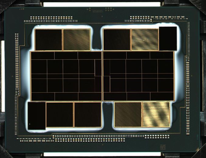
In what’s turning into an Xe sort of day, Intel’s GPU guru and frontman for their GPU division, Raja Koduri, has tweeted that the company is getting ready to begin power on testing for their forthcoming high-end server GPU, the Xe-HPC based Ponte Vecchio. And along with this announcement, Koduri has also posted a somewhat redacted photo of the sizable chip.
Xe HPC ready for power on!
— Raja Koduri (@Rajaontheedge) January 26, 2021
7 advanced silicon technologies in a single package
Silicon engineers dream
Thing of beauty @intel pic.twitter.com/RF8Prsy05f
According to Koduri, Ponte Vecchio incorporates “7 advanced silicon technologies,” likely referring to everything from the four different process nodes used to make the chiplets, to memory stacks, and including the Foveros packaging.
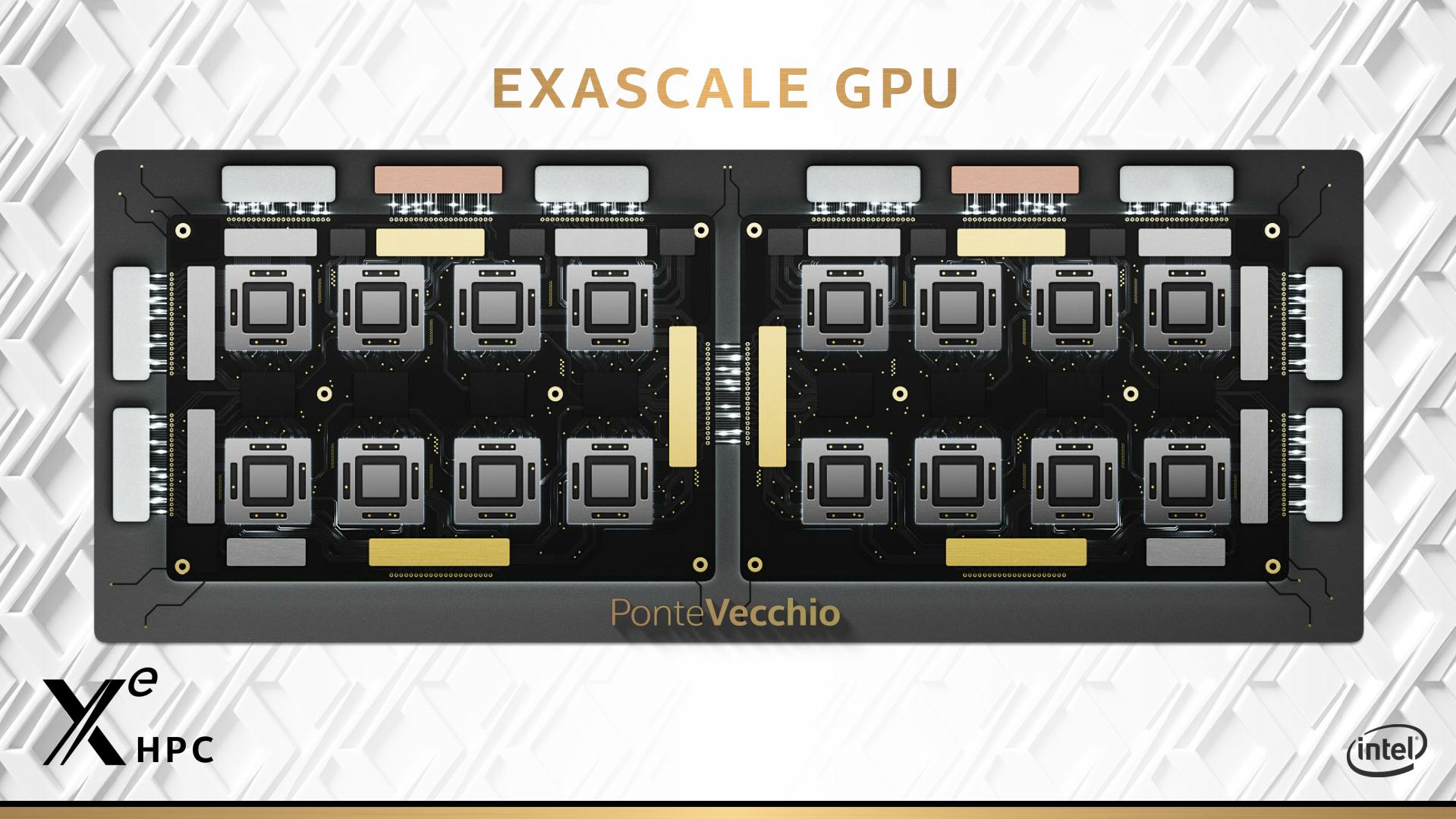
Ponte Vecchio is a keystone project for Intel’s GPU division. Along with being the largest and grandest of their Xe GPUs, the chip will be at the heart of the Aurora supercomputer, Intel’s most recent supercomputer win. So a lot is riding on the chip, and no doubt Intel’s engineers are eager to see a successful power-on test.
Source: Raja Koduri (Twitter)


31 Comments
View All Comments
JKflipflop98 - Tuesday, January 26, 2021 - link
There's a variety of electrical testing (E-test) that goes on during production, but those are only smaller test circuits. The only way to know if the whole thing is going to work after packaging is to actually fire it up and see what happens.nem0 - Tuesday, January 26, 2021 - link
from engineer with some rudimentary grasp of what happens in chips world, to be taken with a lot of salt.A chip is "tested" in the fab after manufacturing in terms of checking whether the "blueprint" that was supposed to be projected onto its portion of the wafer is correct. I think this is where the term yield comes from - what percentage of the wafer contains properly "projected" chips.
However this chip is nothing but a collection of transistors and wires connecting them, and is, as such, an inanimate object. In order to do some meaningful work it needs to be able to interact with the rest of the world which it does over HW lines or programming registers, essentially its inputs and outputs. It also needs power to do all these things.
It is the task of the packaging of the chip (assembly step in the process) to wrap around the chip an environment that will make chip useable.
In case of Ponte Vecchio seems that not one but many chips are being integrated into one package likely with high-speed interconnects. Likely these chips are manufactured in different fabs (including external) so they would need to be shipped to a central location (likely an Intel fab) to integrate them into a package. As a result you get a piece of hardware ready to be plugged in somewhere and tested.
Testing usually happens in an R&D center (California?) after the GPU has been assembled.
What I believe they refer to as power on test is the very first sanity test where the chip is provided with input power and some(many) checks are performed to validate that components are operating properly.
Once this power-on test is done they would likely proceed to do simple generic tests (feeding very simple sequences into the GPU and checking output) and then slowly work towards (much) more complex use-cases.
Hope you get something out of this.
ikjadoon - Tuesday, January 26, 2021 - link
Thanks for the insight.yeeeeman - Wednesday, January 27, 2021 - link
another mention that I would add is that they most certainly already powered it on, they are most certainly well ahead of what they say here...Spunjji - Wednesday, February 3, 2021 - link
Yes, but whether they actually got a fully working chip out of it remains to be seen.JKflipflop98 - Sunday, February 7, 2021 - link
Yield rates are both die level as well as line level. Die level is broken down usually by how many defects per die you run, and line level is how many wafers did you get out at the end vs. how many virgin wafers you started with. Those are optical level inspections.There are also e-test inspections where test circuits built into the part are energized to test various metrics in-line as well as post-process.
We do almost all our testing in Oregon at the Ronler Acres facility.
JayNor - Tuesday, January 26, 2021 - link
Are the 12 chiplets outside the GPUs the Rambo Cache?repoman27 - Tuesday, January 26, 2021 - link
I believe this is a Co-EMIB design with two reticle-limit sized Foveros stacks. Each Foveros module contains 8 XeCU dies (the more or less square ones). The RAMBO caches are the 8 smaller dies in-between the 16 XeCU dies. The 12 dies flanking the XeCU dies on the outside of the modules are the XeMF dies. The four small dies where the two modules abut are probably for the on-package CXL links or whatever I/O they're using between modules. Then there are 8 HBM2E stacks and two transceiver tiles sharing the organic substrate which are connected to the Foveros stacks via EMIB.It seems like the lower die in the Foveros stack may be more like a traditional silicon interposer.
JayNor - Tuesday, January 26, 2021 - link
a previous anandtech article has a diagram indicating those middle 8 chiplets are the Xe-MF.https://www.anandtech.com/show/15188/analyzing-int...
repoman27 - Tuesday, January 26, 2021 - link
Yeah, but Ian made that diagram, and I commented at the time that I thought he got that part wrong. All of Intel’s materials depict the Rambo cache as between the XeCU dies. I’m not sure how much we can really draw from those slides though.