Xbox Series X SoC: Power, Thermal, and Yield Tradeoffs
by Dr. Ian Cutress on February 15, 2021 12:45 PM EST2_waifu2x_photo_noise2_scale_tta_1_678x452.jpg)
This week at ISSCC (International Solid State Circuits Conference), Microsoft presented a talk titled ‘Xbox Series X SoC: A Next Generation Gaming Console’, with hardware engineer Paul Paternoster presenting. The 30 minute presentation covered a lot about Microsoft’s latest console processor, most of which was a repeat about what we saw at Hot Chips in August last year, however there was a new element in this presentation talking about how the console design team balanced acoustics, power, thermal performance, and processor yield, discussing where the hotspots in the design originate and where the performance/power targets of the final silicon were optimized.
Xbox Series X SoC Recap: Project Scarlett
To start, here’s a quick refresher on the processor inside the Xbox Series X, known as ‘Project Scarlett’. Scarlett is a monolithic system-on-chip built on TSMC’s N7 process node. The design has 15.3 billion transistors, measuring 360.4 mm2, with dimensions of 15.831 x 22.765 mm2.
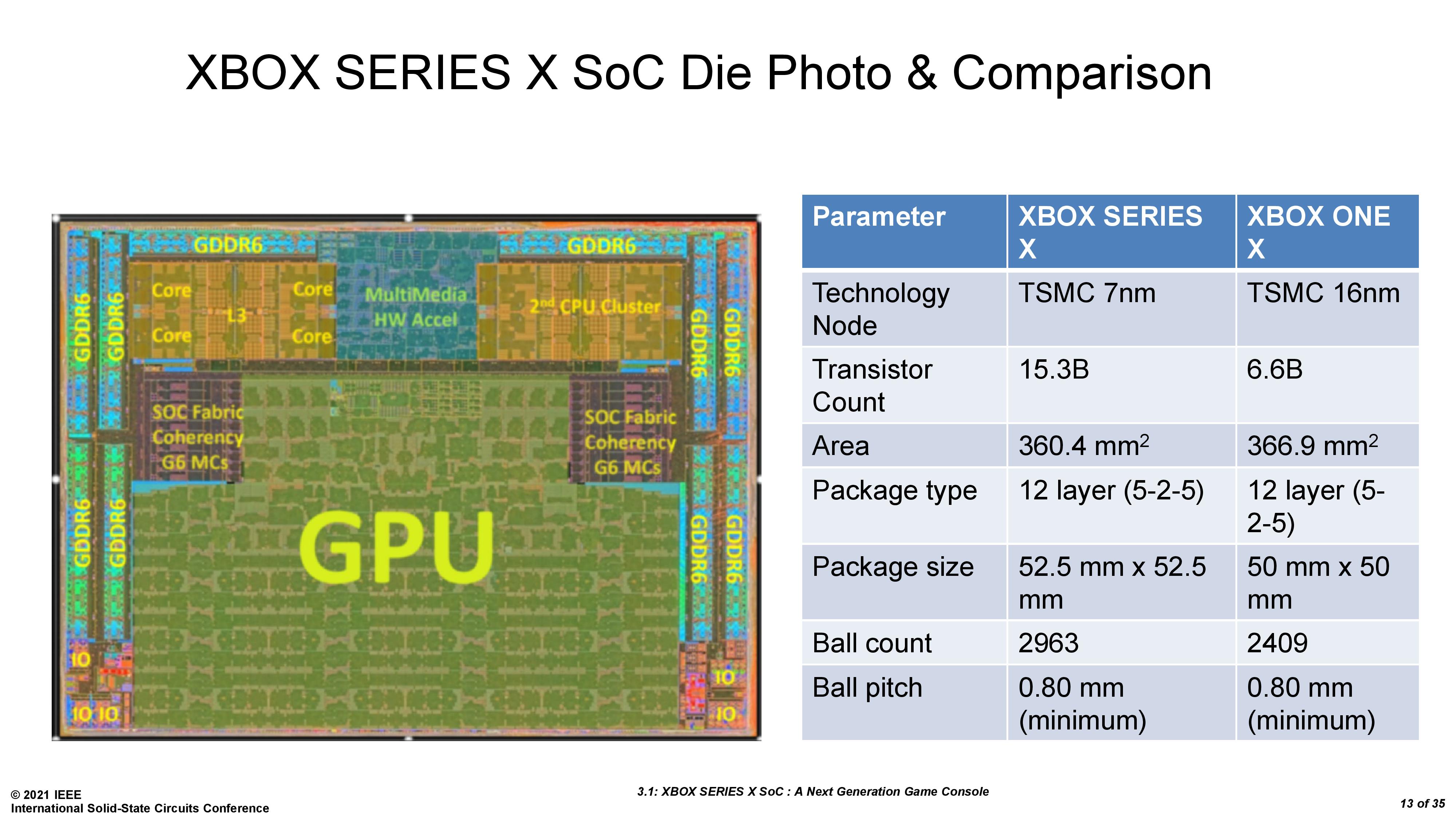
Inside the chip are eight Zen 2 mobile cores, configured into two groups of four cores, each sharing 4 MB of L3 cache similar to AMD’s mobile Renoir/Lucienne processors. These cores are connected through the Scalable Data Fabric to a custom RDNA-based GPU capable of 12 TFLOPS of peak performance, enabling variable rate shading, ray tracing, and other new graphical features. This GPU is built as a 56 compute unit design, however only 52 are used in the final product (more on this later). There is more details on the GPU features in our coverage of the Hot Chips presentation.
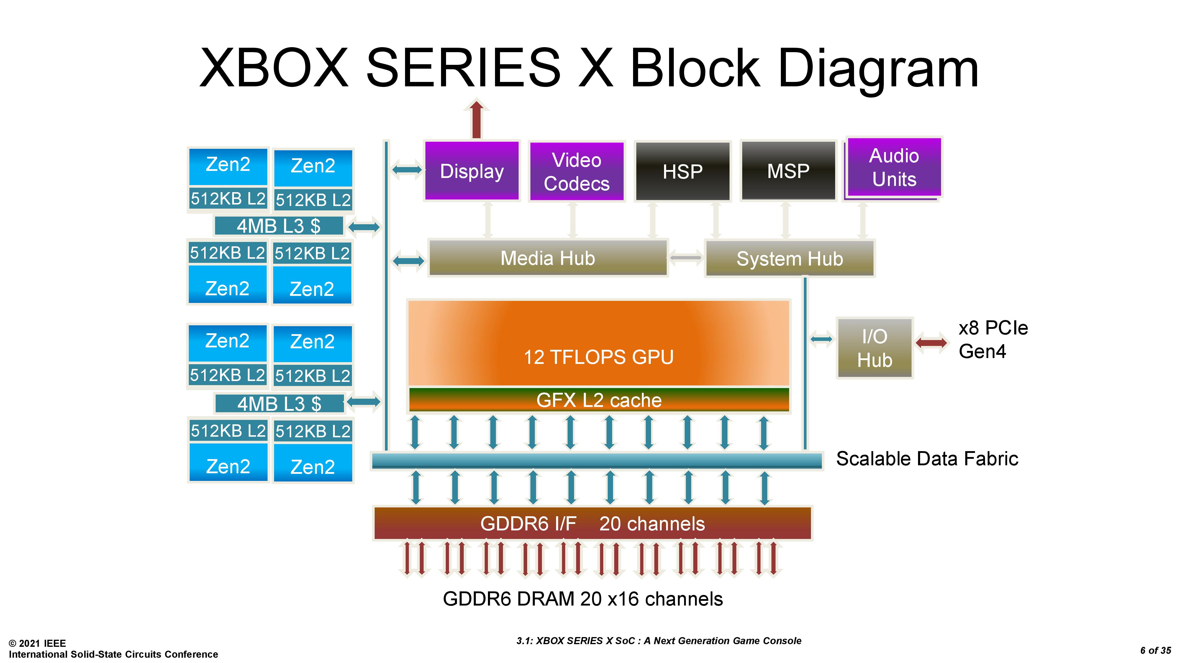
The memory system features 16 GB of GDDR6 through 20 x16 channels. 10 GB of this memory is higher performance, enabling 560 GB/s of memory bandwidth for games, while the other 6 GB is of lower performance, at 336 GB/s of memory bandwidth, for games or circumstances where memory is not the limiting factor. This also enables a lower power state.
The video codec support enables four display planes with 4K/8K AVC encode and decode, HEVC/VP9 HDR decode, and AVC/HDR encode. Three audio co-processors enable compute offload for MOVAD (Opus/Vorbis), CFPU2 (frequency domain processing), and Logan IP for MEC (multi-channel echo cancellation) for removing background noise from microphones.
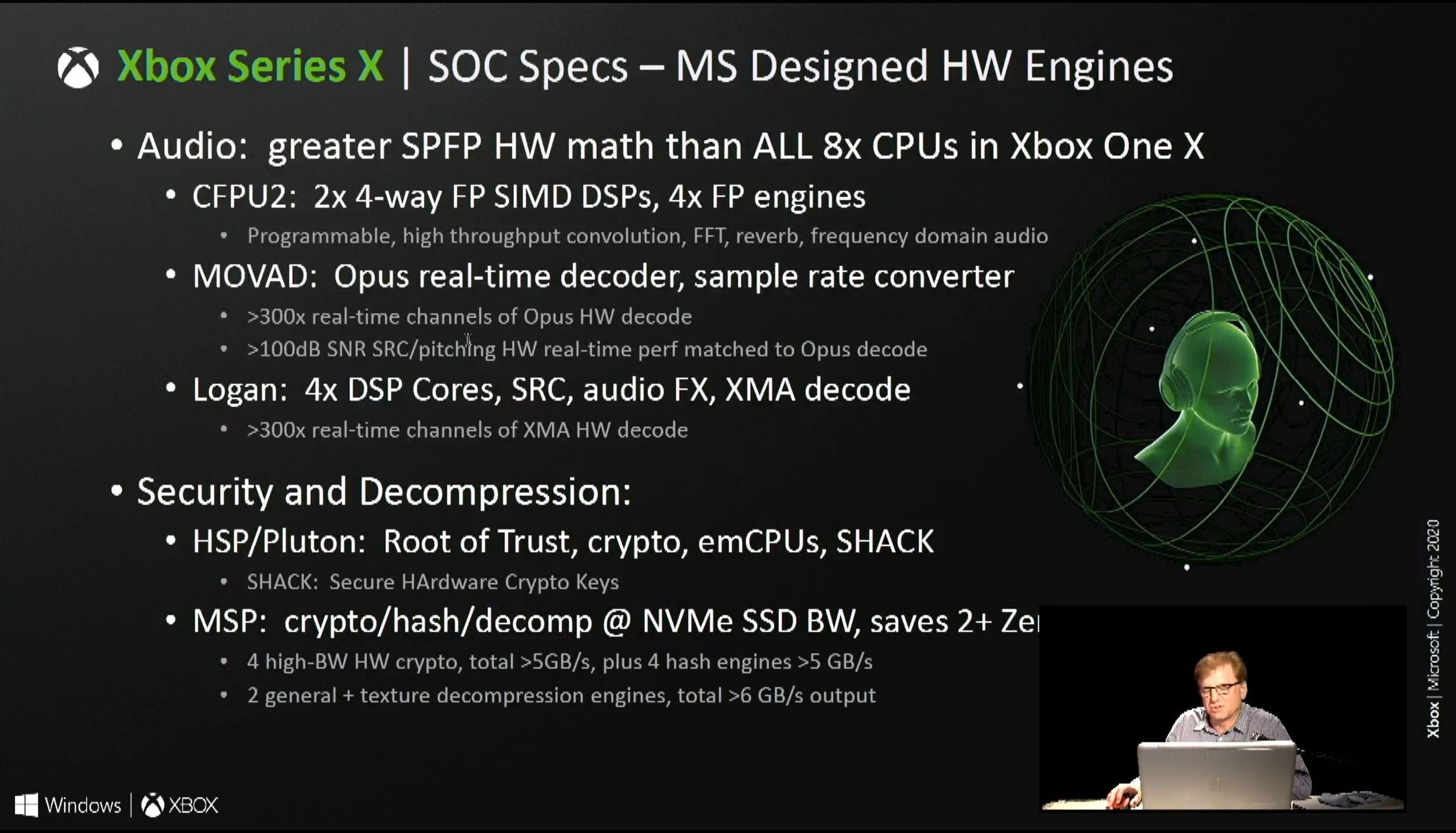
The Hardware Security Processor (HSP) enables root of trust as well as all cryptographic functions, such as secure hardware crypto keys. The HSP is also part of Microsoft’s Pluton architecture, which we will see come to modern CPUs that use Windows over the next couple of years. The Media Streaming Processor (MSP) enables fast encryption/decryption and hashing of external media devices through AES, sufficient enough for the PCIe 4.0 enabled storage on the platform. Microsoft states that compared to the previous generation 7200 RPM drives, its new Xbox Velocity Architecture (using NAND over NVMe plus the MSP) enables faster loading times coupled with 30-35% space savings for games not already distributed in compressed formats.
You can read about the Xbox Series X along with performance and data testing in our review:
For an article dedicated to why NVMe storage matters for these devices specifically as it relates to gaming, and a breakdown of some of the technical details, we have this piece for you:
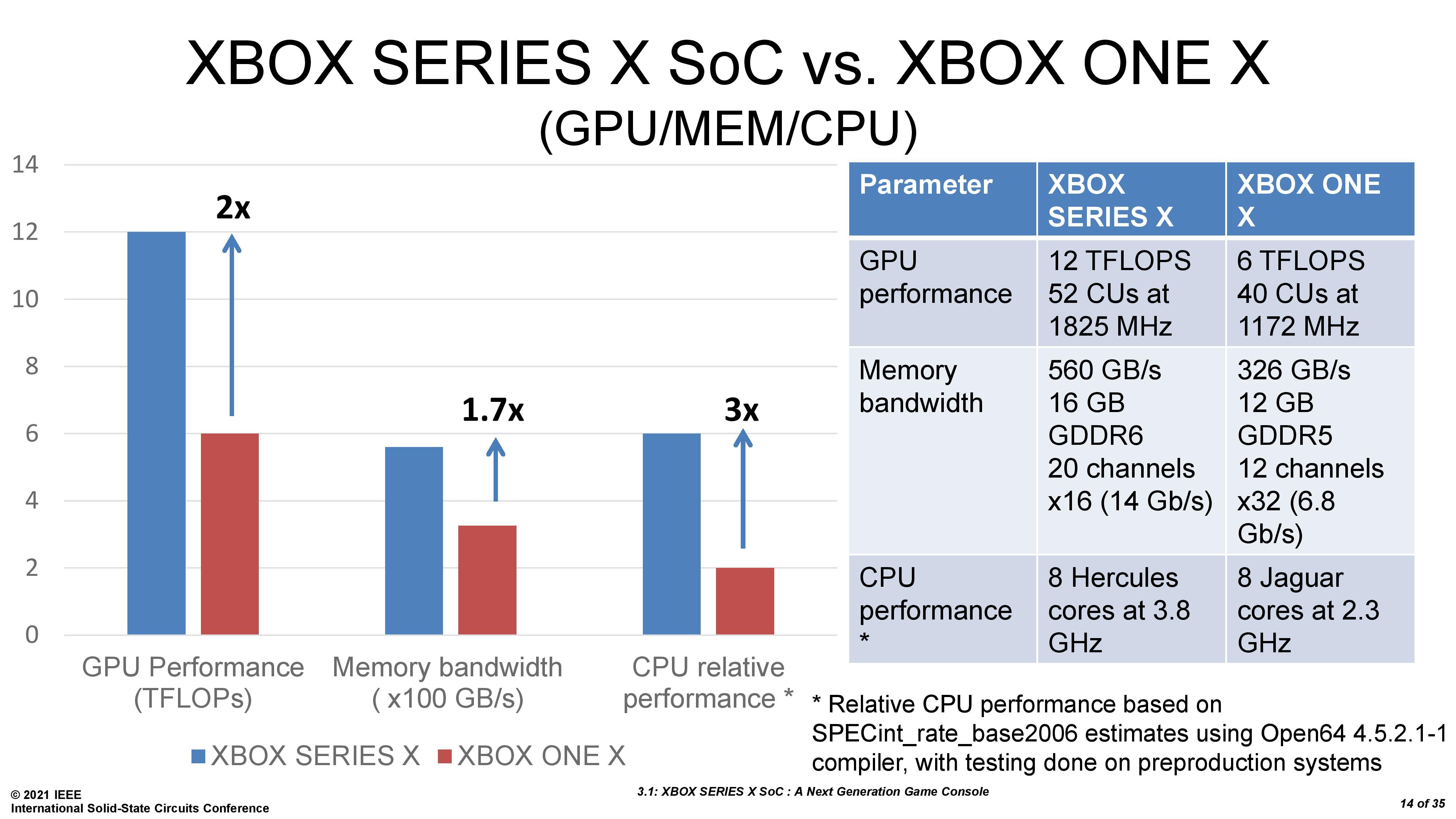
Compared to the previous generation, Microsoft is promoting its new processor as having
- 3x the CPU performance,
- 2x the GPU performance,
- 1.7x the memory bandwidth,
- 2x the IO bandwidth,
- 0.9x the physical volume,
- 2.4x performance per watt,
- Same acoustic performance,
- Stricter compliance for media playback,
All of this, according to Microsoft, was achieved within a +15% power increase compared to the 2013 chip.
We believe the upper limit of the Xbox Series X to be ~270 W, as reported by Eurogamer based on a pre-production sample having a 315 W power supply (and that power supplies will have some headroom). This power number has to cover everything inside the system, so the Scarlett SoC is likely to be a big proportion of that, but not all of it. Microsoft has never given an official number, stating that they won’t provide it without also describing the technical environment the chip is under (from the Hot Chips Q&A). It is important to note that 20 channels of GDDR6 will also consume a portion of that power, so even if the system is 270 W, if we strip most of the system away, the Scarlett chip plus the memory could be 225 W of that. 16 Gbps GDDR6 is often quoted at 2.5 W per chip, and this has 10, suggesting that memory could be 25 W, leaving the SoC with 200 W to split between CPU, GPU, and interconnect.
These are estimated numbers, but if Microsoft would like to weigh in, I’ll gladly update this piece.
With all that being said, in our review of the Xbox Series X, we never saw power numbers anywhere near that high. With an at-the-wall meter, power draw while on the dashboard was 45 W, and the most taxing game (Gears of War 5) only hit 202 W for the full system.
Balancing Acoustic, Power, and Thermals
As with any self-contained system like a console, finding the right balance between power consumption, thermals, and acoustics is a multi-dimensional equation, especially when the updated system is going for more power and the goal is a slimmer system. Paul Paternoster, the presenter in this talk, explained that the goal with the Xbox Series X was to deliver something with 15% higher TDP than the previous generation but have something 20% smaller in volume with the same acoustic performance.
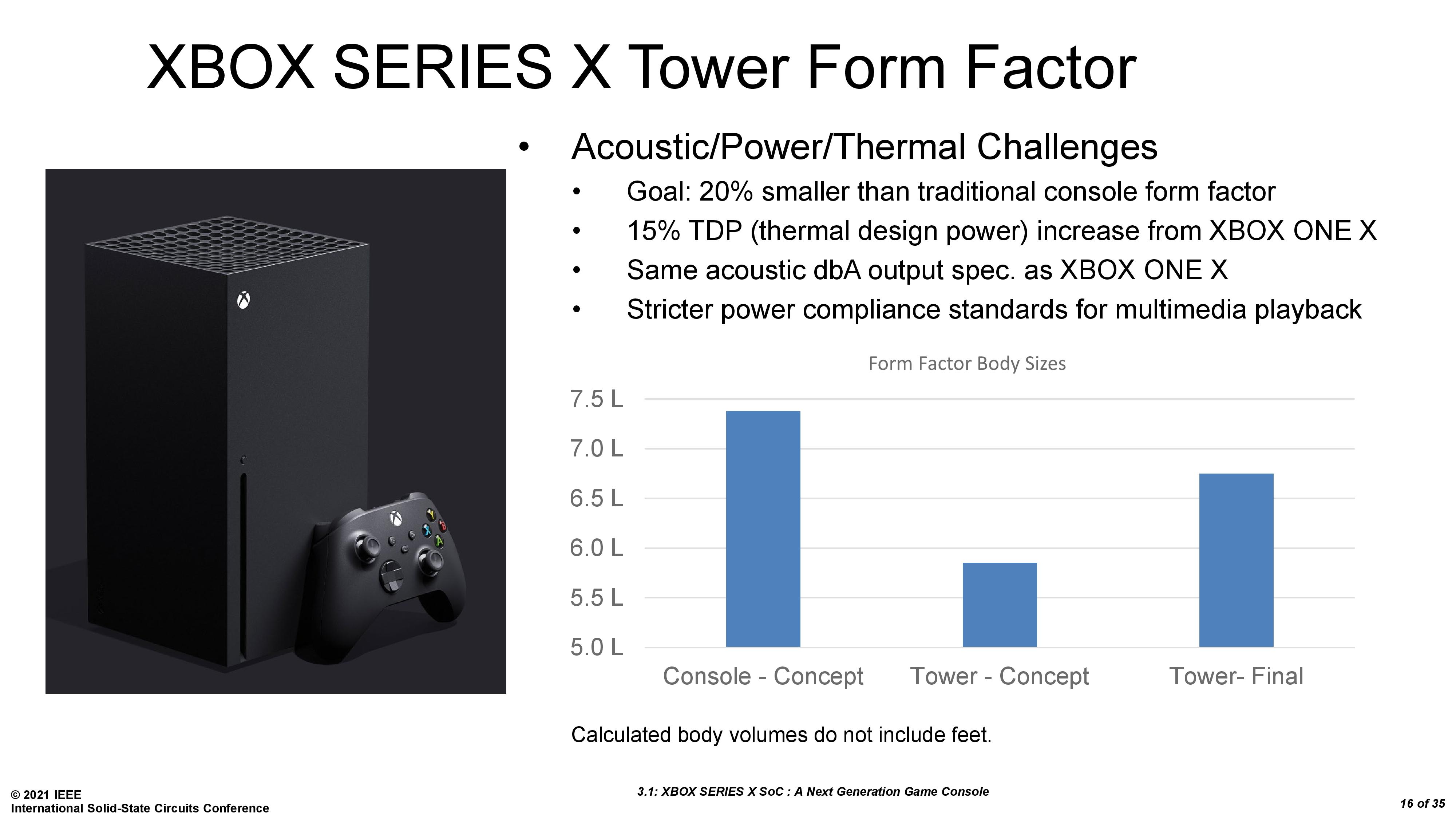
The end result was nearer a 10% smaller volume, but Microsoft enabled a three-channel parallel airflow design combined with a vapor chamber cooler for the main SoC and memory, a center chassis air flow baffle that cools the voltage regulators and other southbridge-related IO, and a custom 130mm axial fan with a 3-phase brushless DC electric motor for high-performance but low acoustic and low maintenance features.
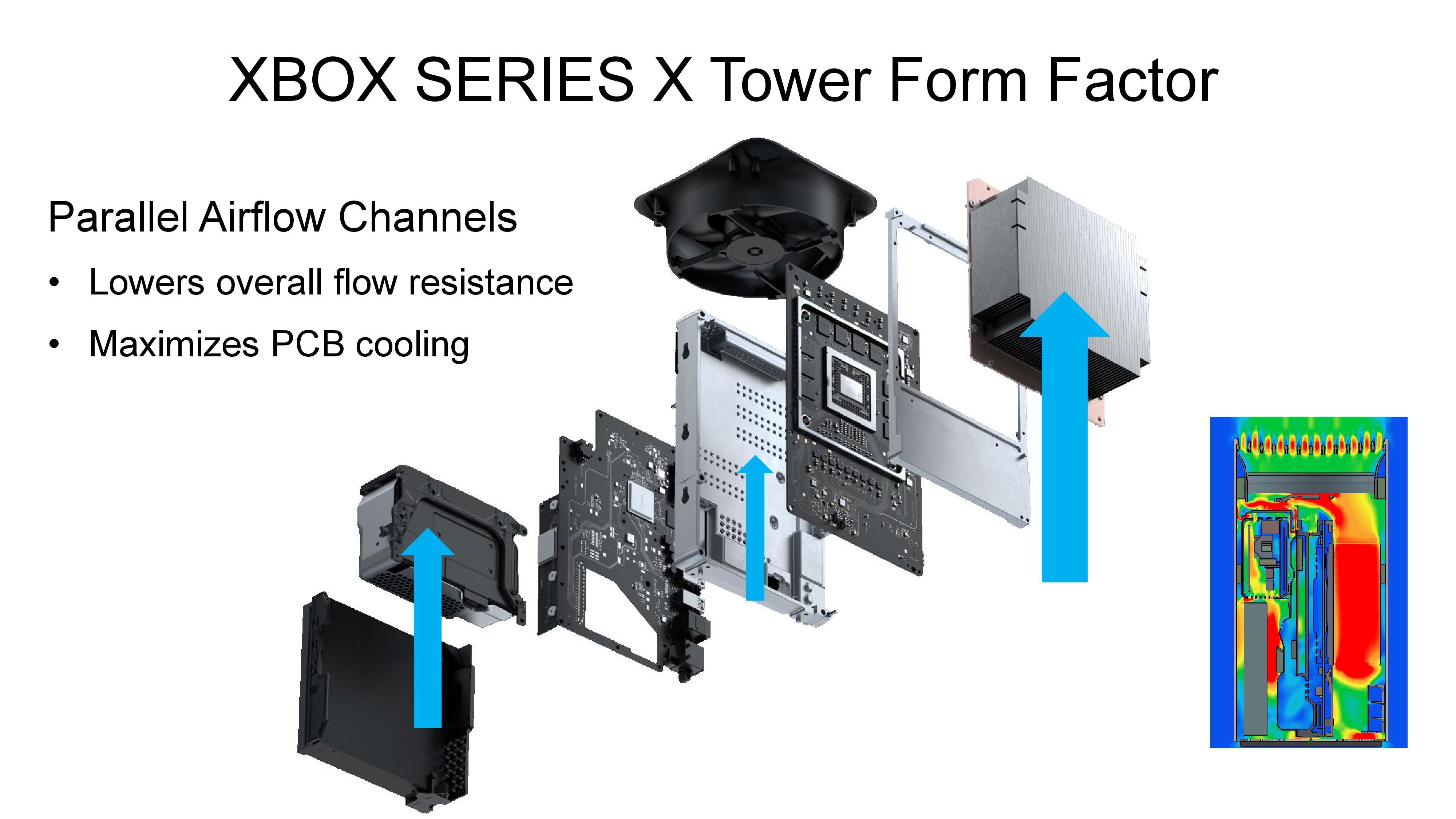
It is worth just zooming in to that thermal simulation in the corner.
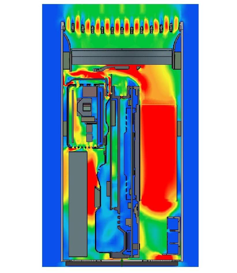
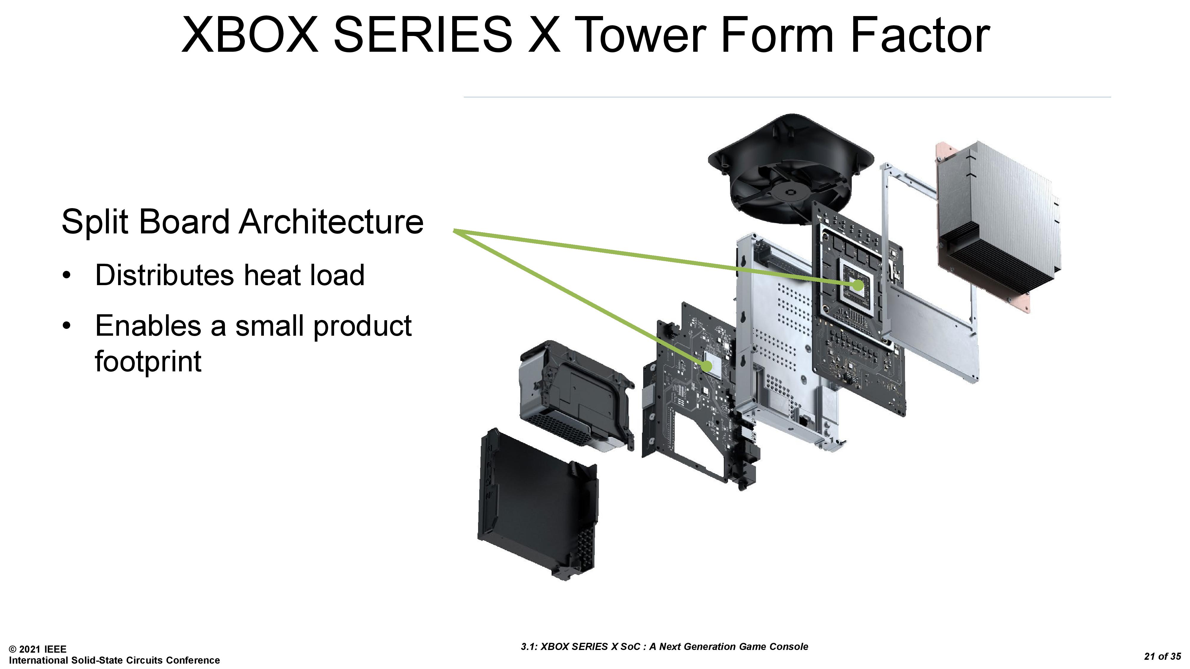
On the right is the main aluminium heatsink for the SoC, then in the middle is center chassis air flow baffle, and on the left is the rest of the system, including the second PCB with the IO. Microsoft split the system into two PCBs, one for the Scarlett SoC and the second for all the IO related connections, in order to distribute the thermals as well as enable a smaller footprint. The only concern with a design like this is the connectivity between the boards often incurs a small power penalty, with a cross board connector with sufficient bandwidth.
Driving Efficiency through Power Management
One of the goals on designing new SoCs is trying to save power in as many different areas as possible. Even small 1% savings here and there add up when you collect a few of them, and Microsoft working with AMD implemented a number of new features. Some of these features we have seen on AMD’s processors already, and few for which Scarlett was the first Zen 2-based SoC to use that feature at the time. Paul Paternoster broke out the power savings into three key areas: power monitoring and regulation (~10%), process optimization (~10-15%), and power state management (operational).
Power Monitoring and Regulation
Under this heading, Microsoft listed a number of features we’ve seen before from AMD, such as digital low dropout-regulators, dynamic voltage frequency scaling, and direct current boot time calibration.
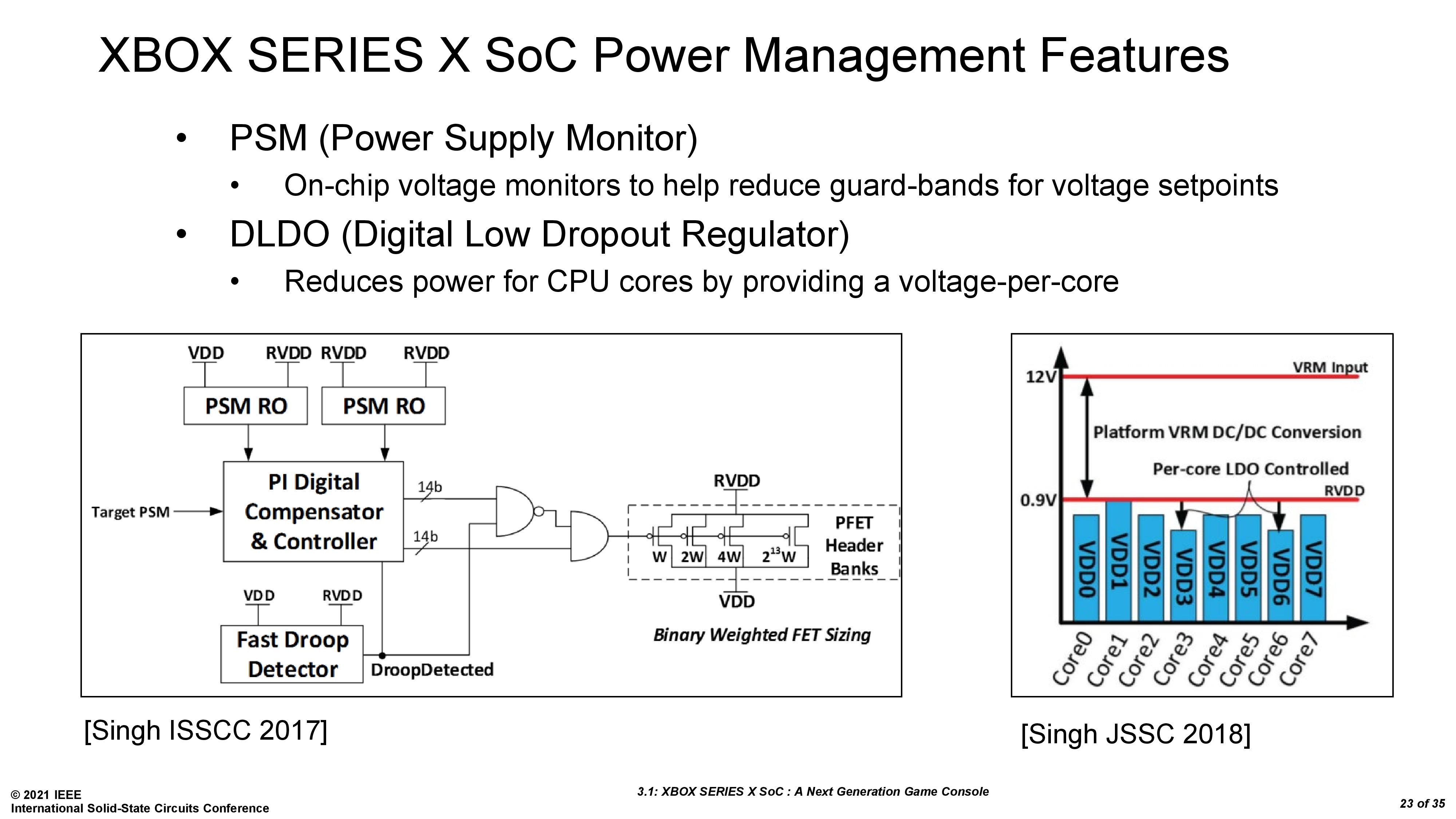
For the Power Supply Monitor we’ve seen this implemented on AMD’s Zen cores since the first generation, providing extra information relating to the critical paths inside the core such that the voltage guard-bands can be optimized for a given workload. This can be used with the DLDO regulators, which provide voltage control on a per-core basis, rather than on a per-complex basis. For context, Scarlett uses a Zen 2 based design similar to AMD’s mobile platform, similar to Renoir, but AMD did not implement DLDO until Lucienne, the second generation Zen 2 mobile product. DLDOs have been on the desktop AMD hardware for at least a couple of generations.
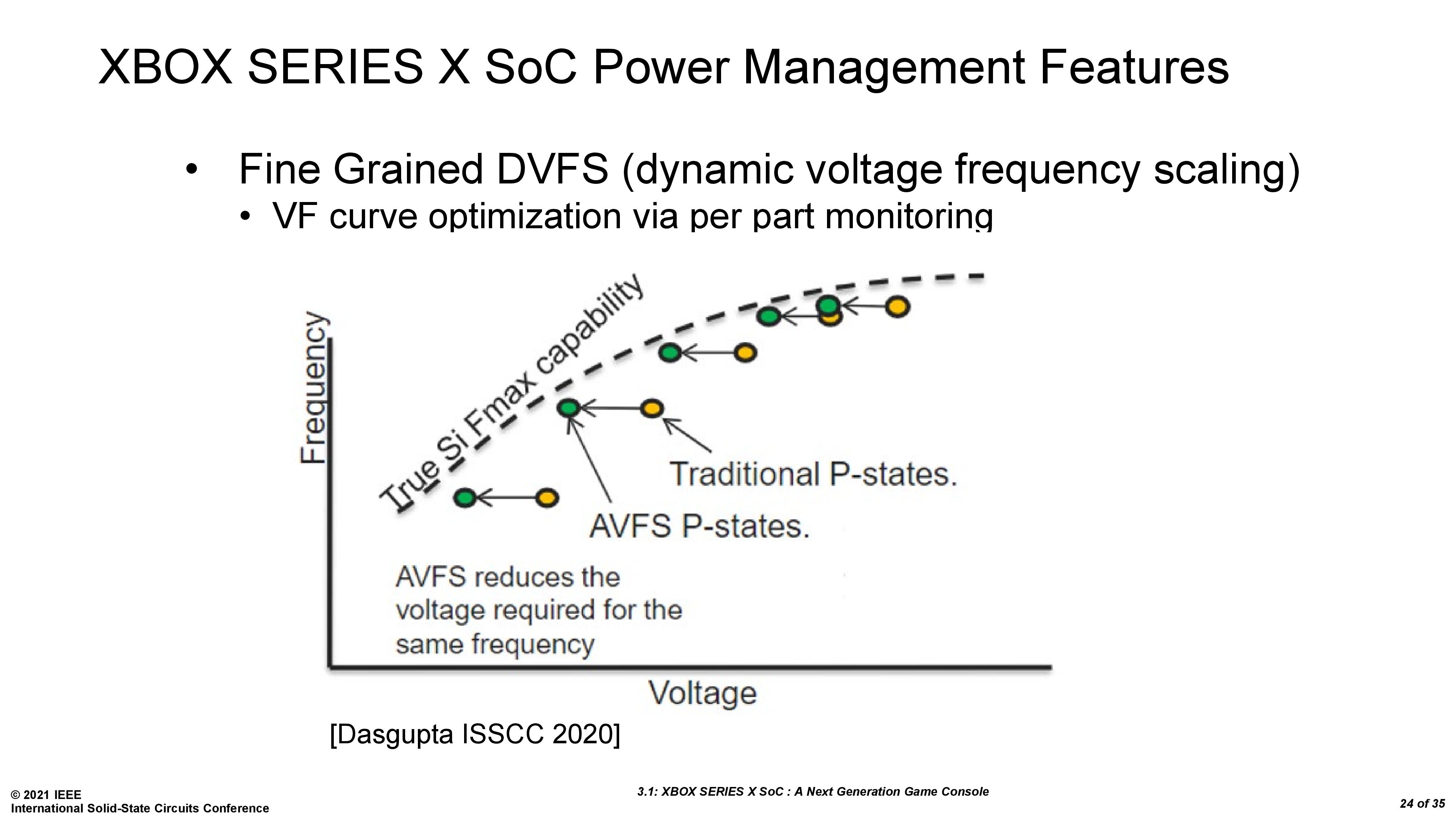
The fine grained dynamic voltage frequency scaling (DVFS) is also another element we’ve seen on AMD Ryzen processors, both in desktop and mobile, enabling finer control of the CPU frequency but also moving the power states lower in voltage closer to the actual silicon minimums. This optimizes performance per watt by lowering that voltage, and combined with the DLDO, it can also be done on a per-core basis. DVFS works best with AMD’s CPPC2 power state control, but as we’ll come to later, consoles rely on fixed power states.
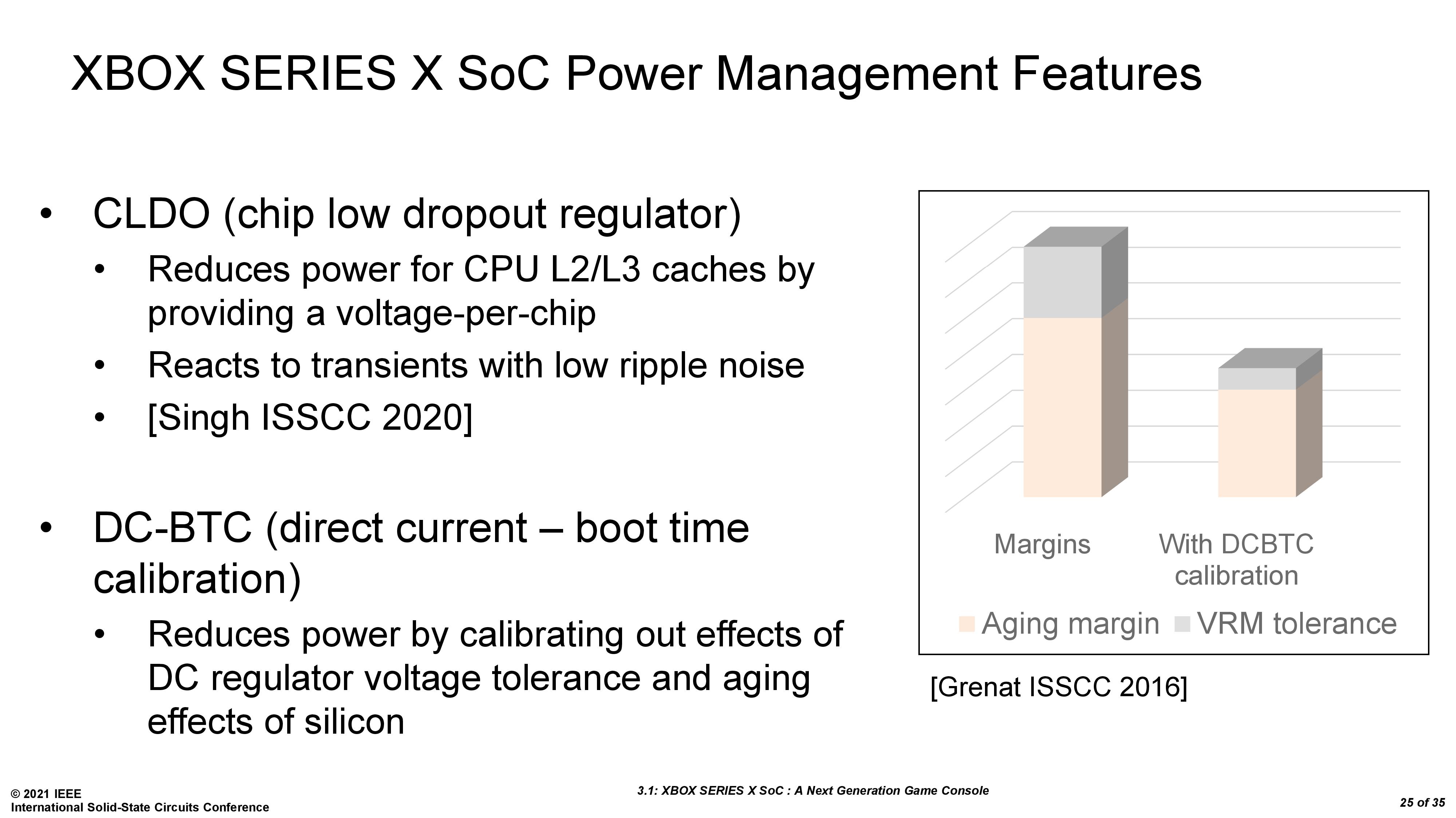
The Chip Low Dropout Regulator (CLDO) is something AMD hasn’t mentioned as part of its Zen processors, but Microsoft is highlighting it here as a way to reduce power to the L2/L3 caches. This obviously becomes more important as caches get bigger – AMD’s desktop processors have 4x the cache compared to the mobile processors and compared to Scarlett. However it seems to make enough of a difference here that Microsoft included it in the talk, although when they say ‘voltage per chip’ I do wonder if they mean per quad-core complex or per-core, rather than a full-chip value.
The last one on this section is DC-BTC, or boot-time calibration of current and voltage tolerance. This was developed during AMD’s Bulldozer days to enable tighter margins for when chips and components age. As components age, due to electromigration and thermal effects, typically higher voltage is required for the same effect. However, without an age control mechanism, an SoC has to artificially raise its voltage from the beginning, called an ‘aging margin’, coupled with high voltage regulation tolerance. The downside of this is that electromigration happens worse at higher voltages, so by doing some form of aging calibration, the chip can have reduced margins, be at lower power, and ultimately live longer due to the lower voltage. This also has a knock on effect to allow a wider range of voltages to be accepted for the final yield given sufficient aging detection and lowering the aging margins needed.
Process Optimization
Alongside implementations on the design side, there are optimizations done at the manufacturing process level. As most of our readers know, manufacturing a processor has 1000 different levers to pull, all of which can change how the other levers operate. Finding the right combination to enable the chip with the best performance, or the best frequency, or the best power, or the best efficiency, all involves finding global or localized minima in the search space.
With the Project Scarlett SoC, Microsoft explained that they implemented two methods at a manufacturing level, both with AMD and manufacturing partner TSMC, to get a better product. Process re-centering starts with defining required voltages and current minimums with respect to frequency and leakage of the transistors.
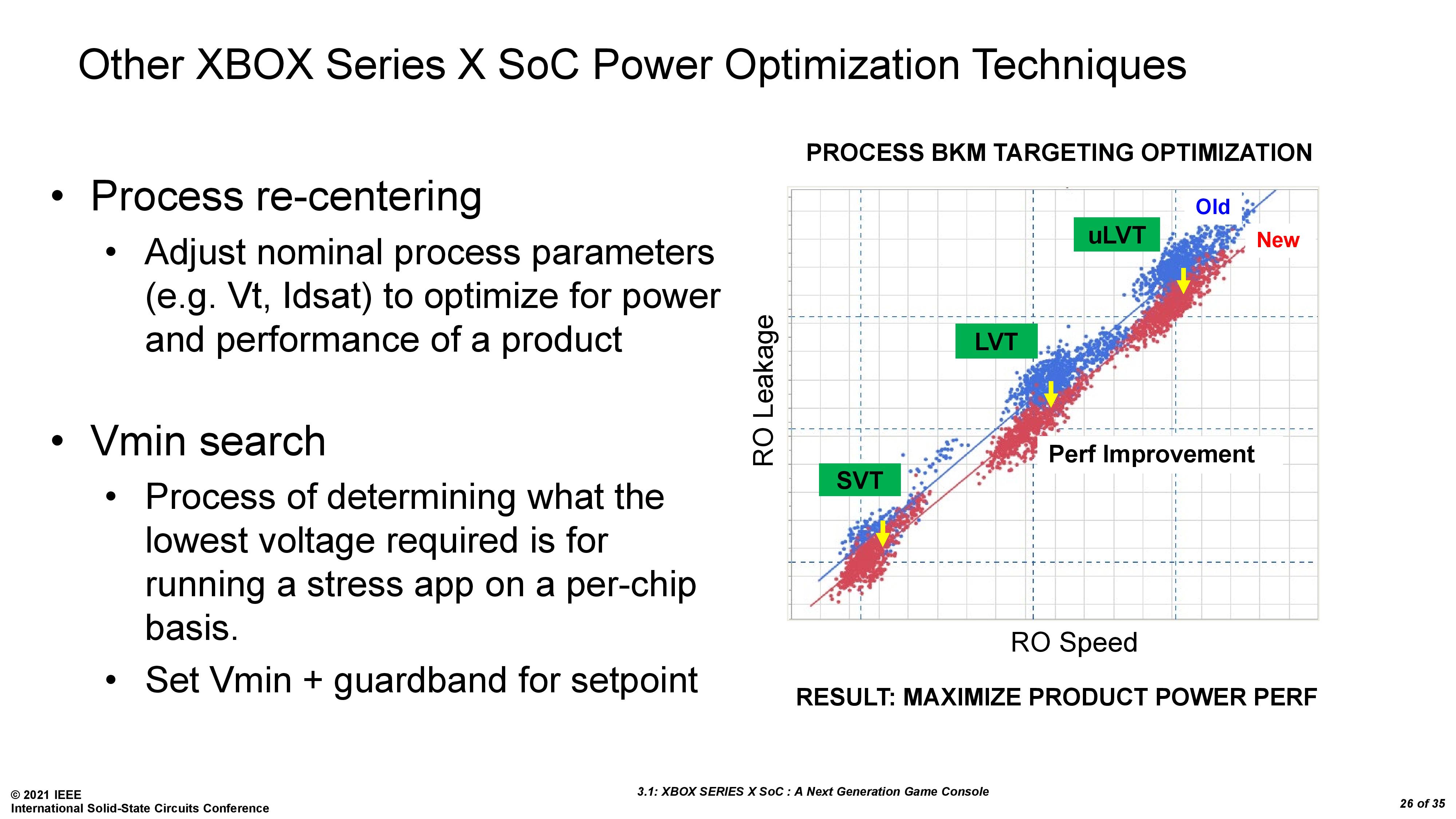
The second part is finding a localized voltage minimum in that defined search space, known as a Vmin search.
Combined these two elements account for 10-15% of the power savings made by the new Scarlett SoC, and these are all manufacturing based optimizations. The depth to which these optimizations might be able to find the best results is often limited by time-to-market (how many search points can you analyze before having to decide on a specific set of values) and how much money is willing to be invested.
Power States
For any given system, enabling a power state provides a window of performance for the system with respect to power, thermals, acoustics, and exactly what performance is needed for the task at hand. Telling a system to run in its peak power state for example will complete any workload as quick as possible, at the expense of power, thermals, and acoustics.
A modern desktop PC will often vary the power states on the fly, and AMD’s CPPC2 technology allows these power states to be a continuous flow for when performance is requested. Consoles on the other hand can’t use this because of the nature of how the system works with game developers.
Microsoft defines a number of power states in the system in order to give the right performance for gaming, for video playback, for downloading game updates, and for other features. Each part of the system can have its own set of power states:
- The CPU has 8 power states
- The GPU has 5 power states
- The internal fabric has 4 power states
- The GDDR has 3 power states
Microsoft uses these bands to create specific console operating modes, enabling developers to work and optimize for a given power and performance, rather than the moving target of modern PCs. On these console games, obtaining 30 FPS minimum at 1920x1080 resolution is essentially the minimum bar, and if a developer knows that the system will have a guaranteed performance level, they can tune to those performance numbers.
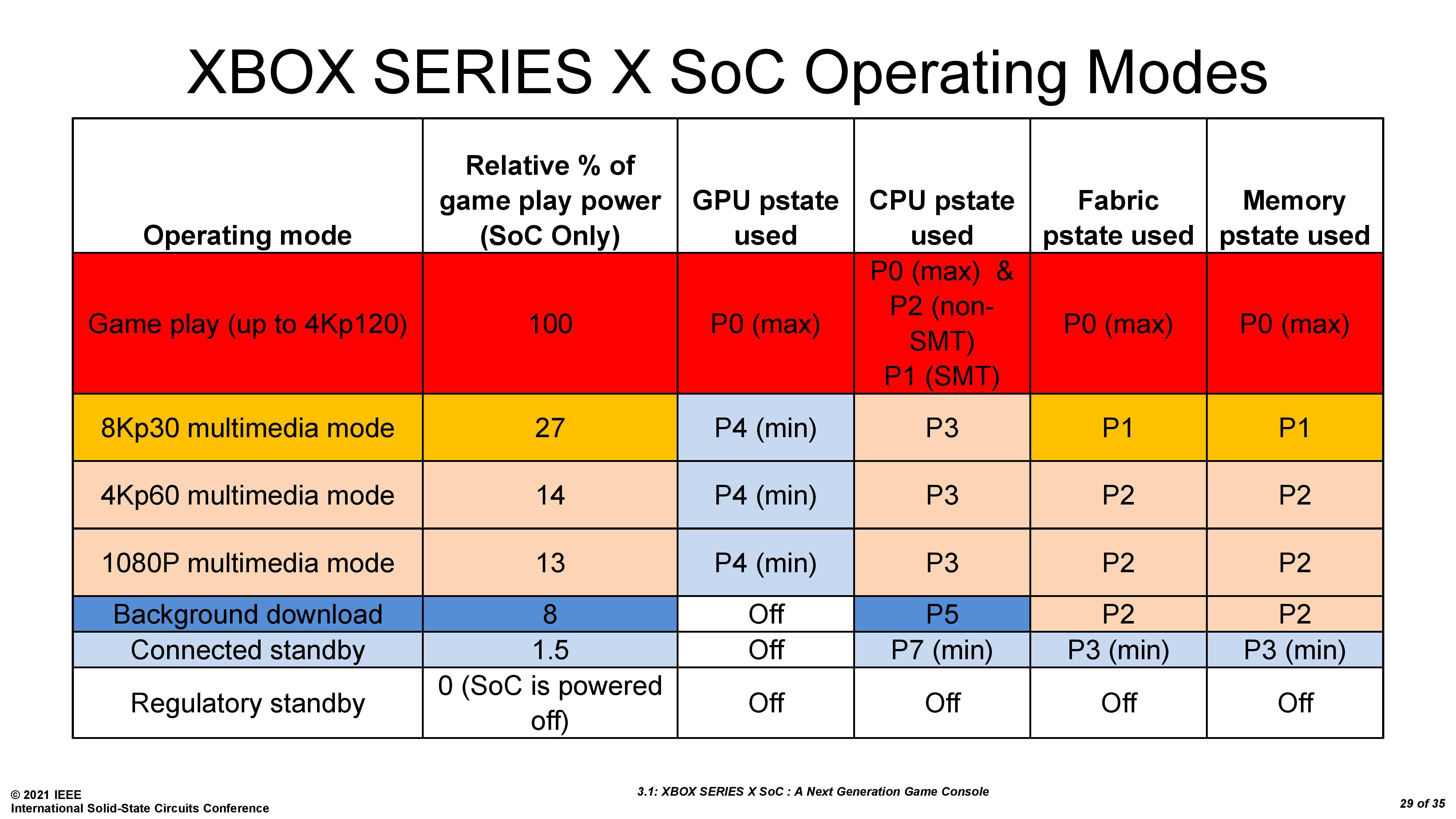
Here are the operating modes that Microsoft is telling us about – there may be more. In game play, every power mode is set to the maximum, so the system gets full access to all the performance necessary. In video playback, the console will be in a number of different operating modes based on the format of the content, and then there are some lower power modes for background and connected standby. There may be other power modes aside from these, such as for 2D or indie games, or if the system detects that certain performance levels are not required.
Solving for Thermal Density and Yield
Thermal Density
One of the elements of the ISSCC talk by Paul Paternoster related to how different this generation was for thermal density measurements compared to previous console generations. In the past, as Paul explained given that he has worked on several generations of Xbox processors, the GPU is often the limiting factor in thermal density, which limits the acoustic characteristics of the platform. The GPU often has the high performance demands, and has historically been where the hot spots are. Paul noted that for the Xbox Series X SoC, things are different.
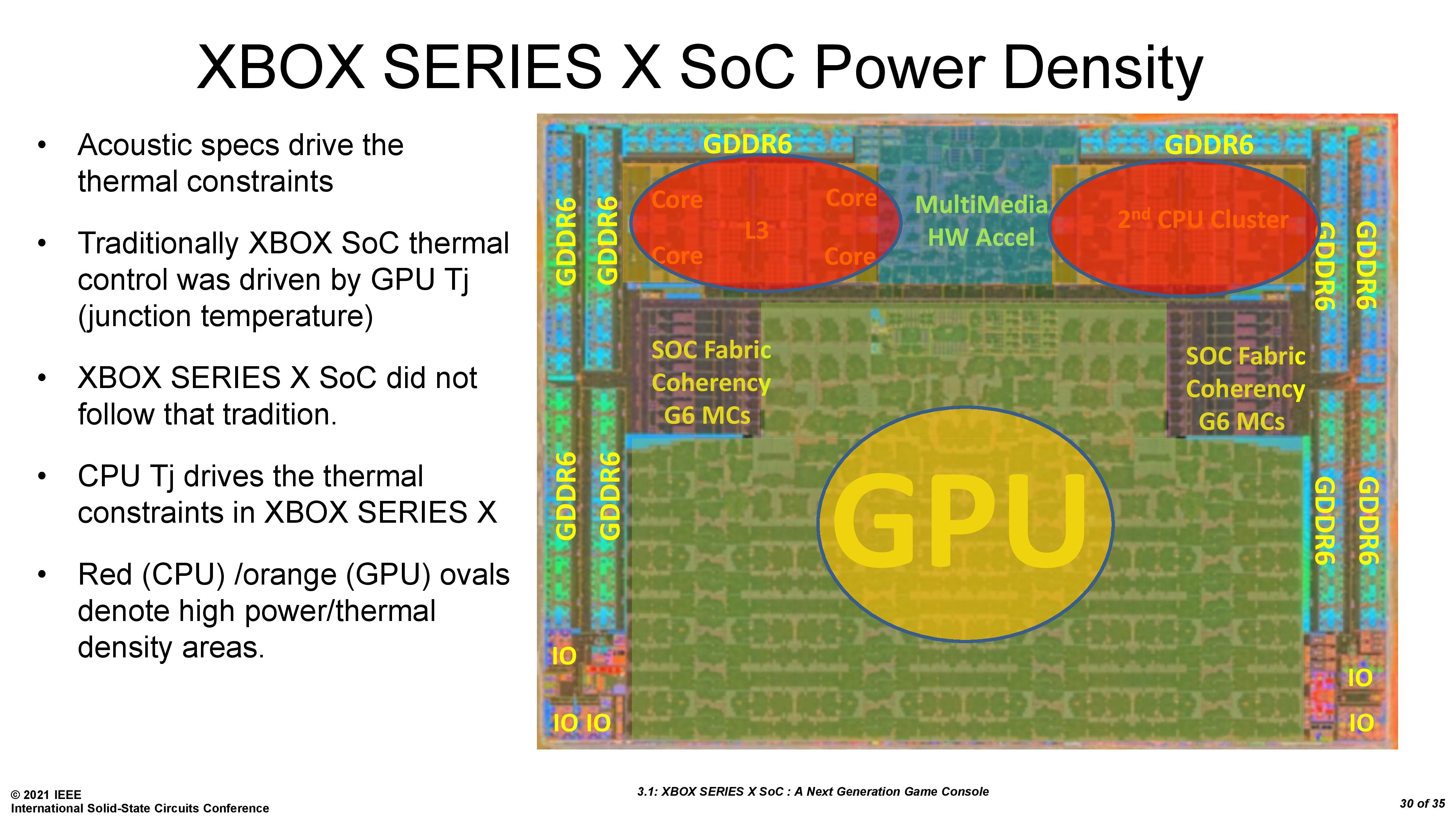
For Scarlett, it is actually the CPU that becomes the limiting factor. Using AMD’s high-performance x86 Zen 2 cores, rather than the low power Jaguar cores from the previous generation, combined with how gaming workloads have evolved in the 7 years since, means that when a gaming workload starts to ramp up, the dual 256-bit floating point units on the CPU is where the highest thermal density point happens.
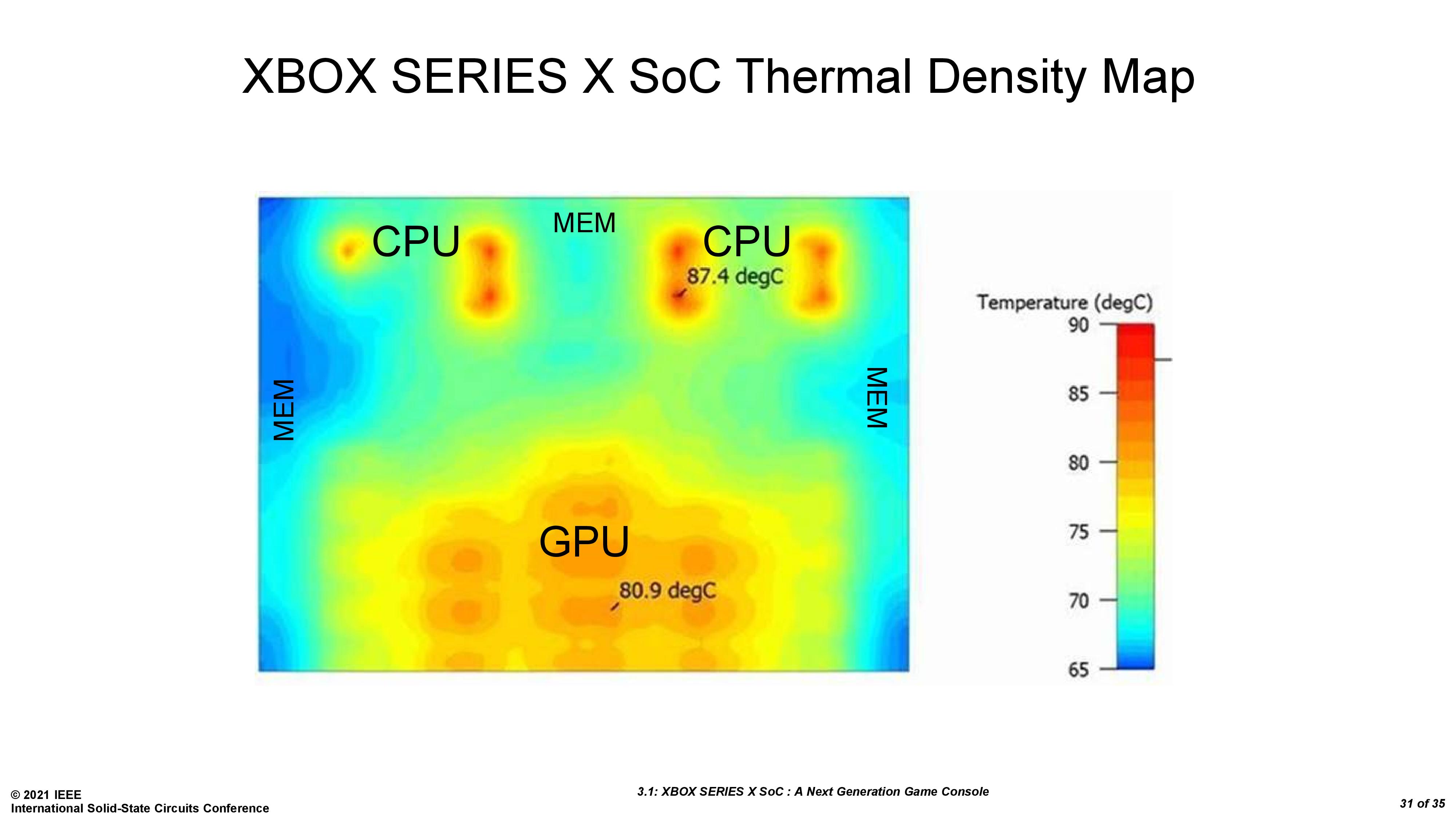
In this slide shown, although it doesn’t indicate what sort of workload is in play here, whether it is an active game or a power virus, Microsoft is showing 87.4ºC at the hotspot on the CPU side, while the GPU only has a 80.9ºC hotspot. Now this also comes down to the frequency choice and design point of the hardware, and finding the right balance between CPU power, GPU power, and overall thermal characteristics and acoustics.
Microsoft stated that because of this difference and now the CPU was the thermal hot spot, the acoustics now center around that point. As a result of Microsoft’s testing, the company is stating that the CPU is disproportionately responsible for the acoustics of the design: every additional Watt the CPU uses is worth five times more to the acoustic budget than the GPU.
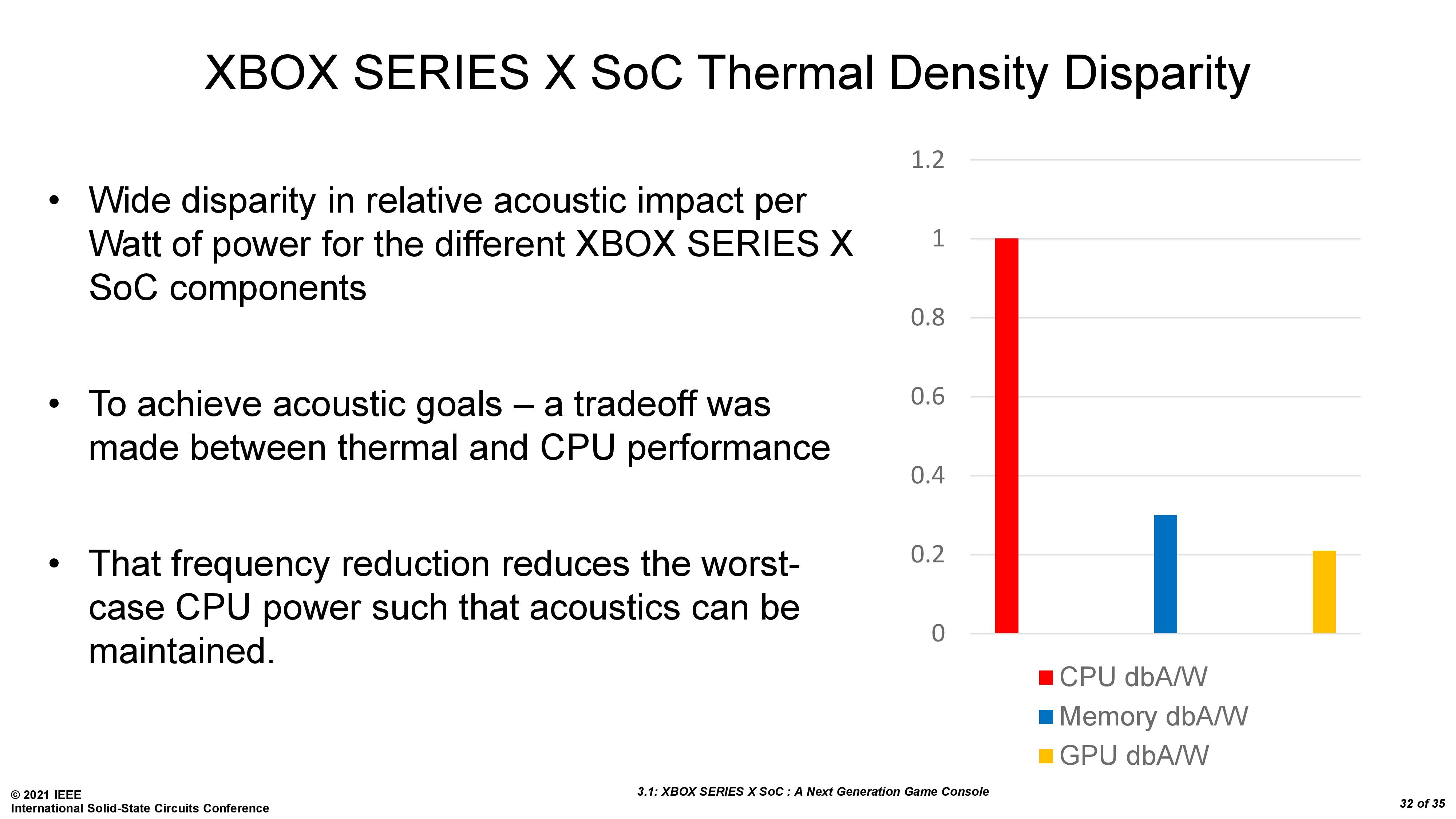
It’s an interesting point I hadn’t considered, but it means that in order to meet the desired goals, Microsoft spent time optimizing for the right CPU frequency, making the tradeoff between performance and thermals. This is also why the system runs at 3.6 GHz when simultaneous multithreading is enabled, but can go higher to 3.8 GHz when simultaneous multithreading is disabled.
Solving for Yield: The Effect of the GPU
Console processors are different to desktop and mobile processors in the sense that there is no SoC binning. For any given silicon product that is manufactured, there will be both a variability in transistor performance as well as defined defects in the design. The goal of the manufacturing process is to provide the best of both, naturally! For a given design, consumer processors in PCs and laptops will be put into different ‘bins’ and assigned different names and values based on transistor performance. Console processors by contrast have to all perform the same in order to meet a minimum performance requirement, and there is no binning. A console manufacturer has to use a design and a performance point such that as many processors as possible from the production line meet that point. This is part of the yield equation for any console processor.
We’ve covered above a number of design choices that Microsoft made in this article, some of which factor into that binning equation and making sure the design gets the highest yield possible. One other factor we haven’t specifically touched on yet is the GPU. The Scarlett SoC physically has 56 compute units for graphics, but only uses 52 in the retail product. The presentation at ISSCC spent some time going into the upsides of both options, but ultimately why Microsoft went with 52.
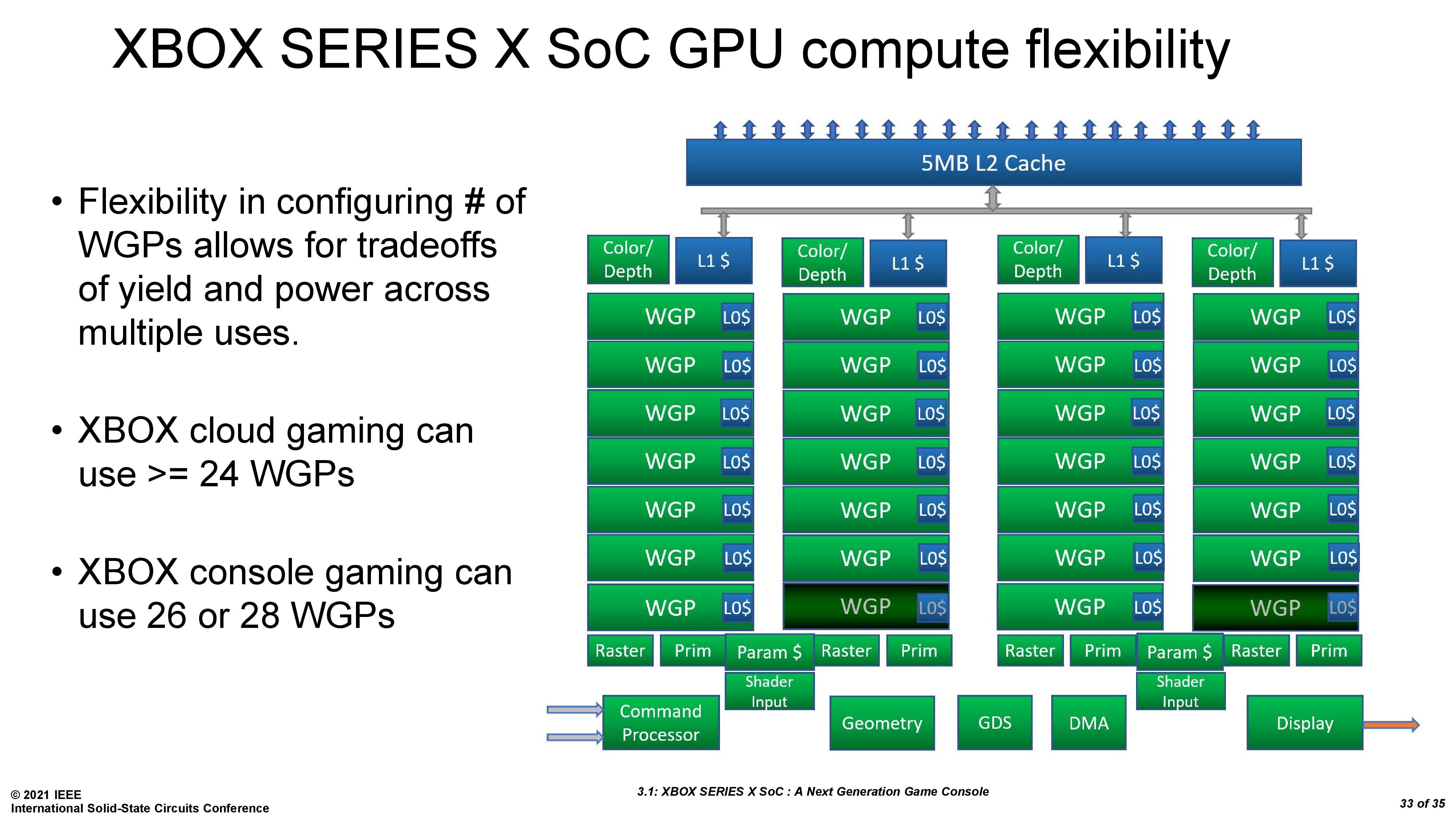
Microsoft here talks about Work Group Processors (WGP), which contain two compute units and some shared resources. This means that the full chip design has 28 WGPs.
Paul Paternoster explained that from chips coming off the production line, a substantial number could run with all 28 WGPs enabled. The goal of the graphics was to provide 12 TFLOPs of performance, and so by some simple math, Microsoft could do either of the following to hit that number:
- 28 WGPs enabled at 1675 MHz
- 26 WGPs enabled at 1825 MHz
Both of these configurations enable 12 TFLOPs. Because the frequency of the 28 WGP design is lower, this also enables a lower voltage, combined for an overall power saving of 20% if all 28 WGPs are used.
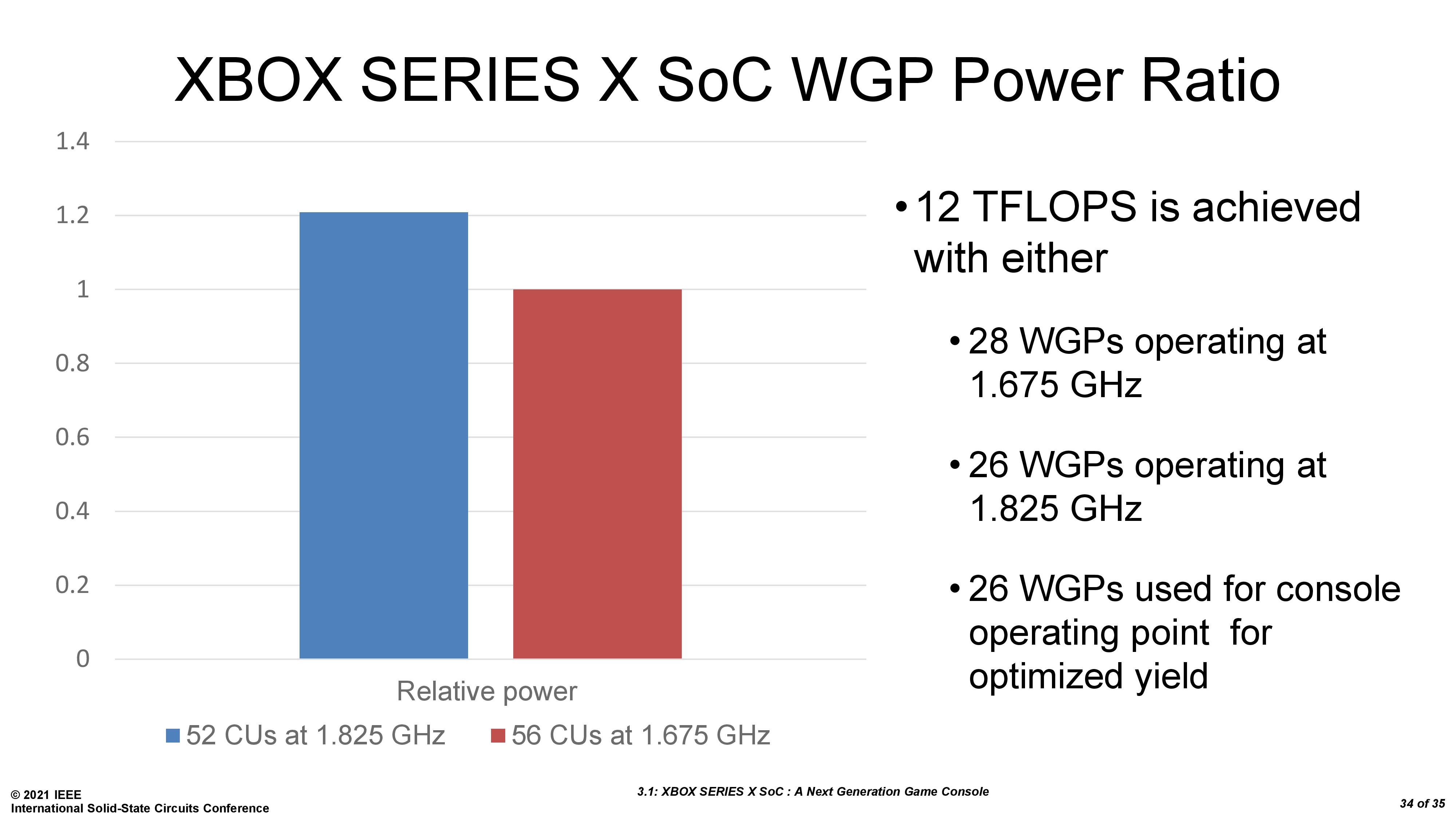
Of course, a 20% power saving is quite substantial, as it would either enable better performance per watt, or enable higher performance. But the issue is that not enough processors were coming off of the production line with all 28 WGP running at this frequency. The variability of the processors, due to both transistor performance and defects, meant that 28 WGP versions didn’t make sense financially.
Microsoft is using TSMC’s best DUV-only 7nm (N7) process node, which has been stated as having a defect rate of 0.09 defects per square centimeter.
- A 300 mm wafer has 706.86 cm2 of area
- A defect rate of 0.09 defects per cm2 means ~64 defects per wafer
- Scarlett is 360.4 mm2 (15.831 mm x 22.765 mm)
- Note that SoCs are rectangles, and wafers are circular,
- Wafer die calculators show that 100% yield of this SoC size would give 147 dies per wafer
- Microsoft sets the frequency/power such that if all dies are good, all can be used
- With a 0.09 / cm2 defect rate, there are 107 good dies per wafer
- This means a 73% yield, 107 / 147
Assuming a defect happens in one of the GPU compute units or WGPs, which is a very good chance because the GPU is the biggest part of the processor, by absorbing that defect and disabling that WGP, that SoC can be used in a console and the effective yield is higher.
When the defect rate is 0.09, which is nice and low, the chances that two defects occur on the same chip are very small. Even then, by choosing to run a design with only 26 WGPs enabled, two less than the full 28 WGPs, almost everything that comes off the manufacturing line can be used – an effective yield increase, reducing the average cost per processor by a third.
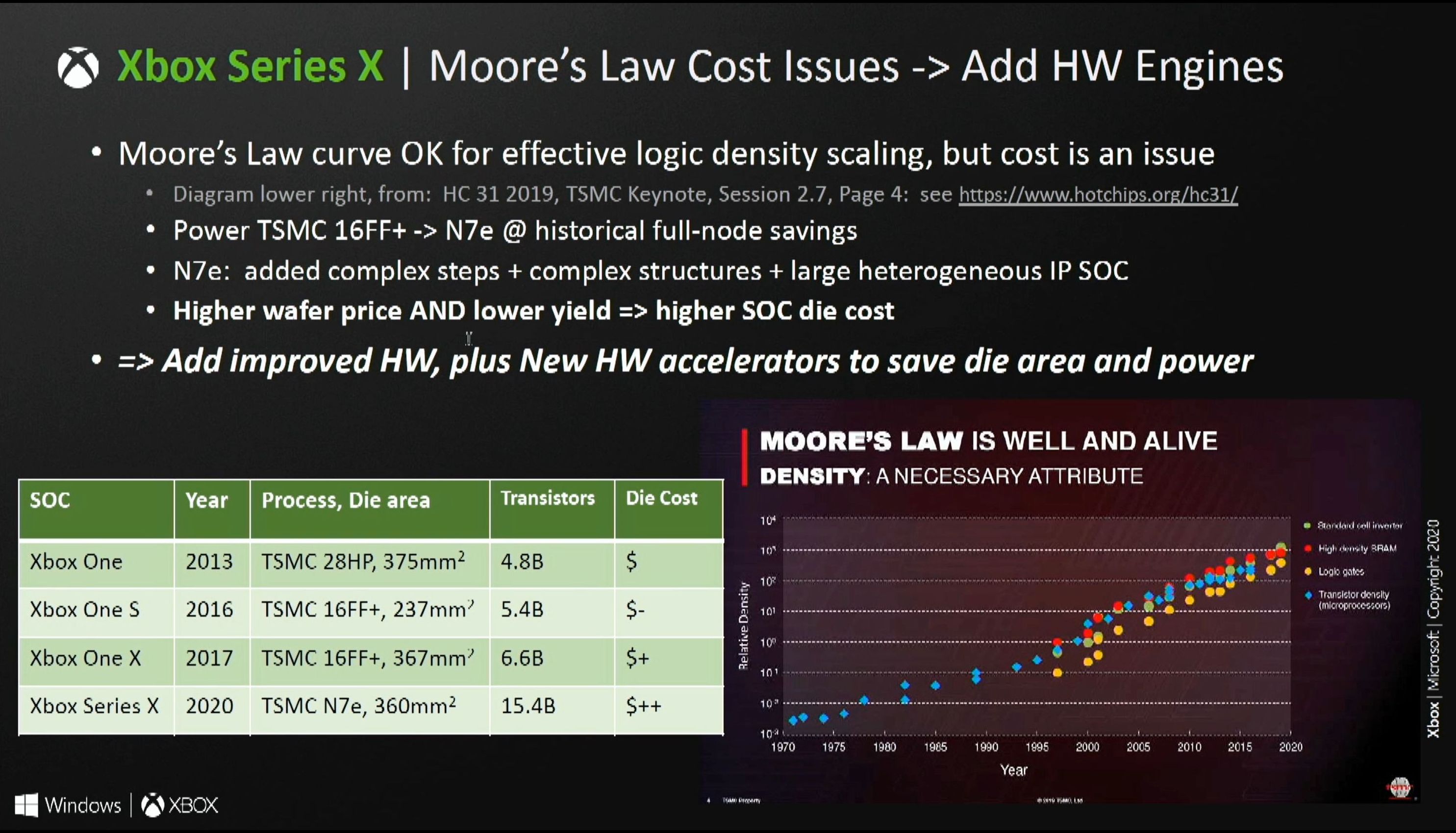
Microsoft has already explained that the cost of the processors for this generation of consoles is a lot higher than the Xbox One X in 2017 and a lot lot higher than the Xbox One from 2013. This comes down to having roughly the same die area, but on a more advanced process node, more complex steps and structures, large IP blocks (some of which may be licensed), higher wafer price, and lower yield.
So the opportunity to reduce the cost of the processor by up to a third, at the expense of a 20% power tradeoff in the GPU for the same performance, isn’t a bet to be taken lightly, and no doubt a number of engineers and bean counters would weigh up the pros and cons. Different design departments may have chosen to go in the other direction.
One knock-on effect however with the 26 WGP design choice is that it means more SoCs are manufactured in a given unit of time, enabling more units to come to market in a timely manner, which is especially important if your product is flying off the shelves and more need to be made (such as the situation today). Looking for numbers on exact sales figures for the Xbox Series X is relatively difficult - most quoted numbers combine the Series X it with the smaller Xbox Series S. From a number of different sources, that number for combined sales is ~3.5 million, and based on advice from GamesIndustry.biz, the Series X devices make up around two thirds of all units. This would make the Series X sales around 2.33 million CPUs, suggesting a minimum of 16000 wafers total at 100% yield, or up to 21800 wafers at 73% yield. The real number is likely to be somewhere between the two, but you can see how much of an effect the configuration choice can have on getting product to market in time, as well as the cost per processor.
Source Material: 68th ISSCC, Feb 13-22nd 2021


81 Comments
View All Comments
Steinegal - Tuesday, February 16, 2021 - link
And it is not even 7200RPM drives in the One X it is 5400RPM it is a pain.Jorgp2 - Tuesday, February 16, 2021 - link
Some QLC drives are slower than an SMR HDD.Also, the SSD in the Series X is pretty much bottom of the barrel.
GeoffreyA - Monday, February 15, 2021 - link
Interesting reading. Thank you.arjuntare - Monday, February 15, 2021 - link
16 Gbps GDDR6 is often quoted at 2.5 W per chip, and this has 10, suggesting that memory could be 25 WShouldn't it be 8 chips, 20W ?
IanCutress - Monday, February 15, 2021 - link
There are 10 GDDR6 controllers supporting 20 x16 links, with 10 GDDR6 chips. Not eight. Google for images of the Xbox Series X SoC to see that there are 10.SolarBear28 - Monday, February 15, 2021 - link
Fantastic stuffeastcoast_pete - Monday, February 15, 2021 - link
Thanks Ian, great overview! One thing I am wondering about is whether the twenty-some percent of "defective" chips end up in the Series S, after some laser surgery, of course.Another recurrent thought of mine is that I wouldn't mind this configuration as my Windows 10 desktop machine. I am pretty sure this SoC is locked down against such diversion, but if anyone has tried and was successful, I'd really like to know how it's done.
IanCutress - Monday, February 15, 2021 - link
Well that 73% is probably the lower bound of actual yield. They might use any other chips in the cloud services. The Series S uses a completely different die design, so it's unlikely they'd use this chip for that.We tested the previous Xbox One SoC a few weeks ago. So you might be waiting another 7 years for this one to come to Windows. https://www.anandtech.com/show/16336/installing-wi...
diehardmacfan - Monday, February 15, 2021 - link
It might not be the best use of your time but it would be awesome to get some input from you on all the "Is it RNDA 1 or 2" speculation going around right now.IanCutress - Monday, February 15, 2021 - link
My input is zero. It is what it is. It's not as if there's going to be a variant in a few months with more features. Consoles are quite static, and if they do have a cost reduction model, it's difficult to see where they'd go when the next manufacturing jump is to EUV, which undoubtedly costs a pretty penny.