IBM Creates First 2nm Chip
by Dr. Ian Cutress on May 6, 2021 6:00 AM EST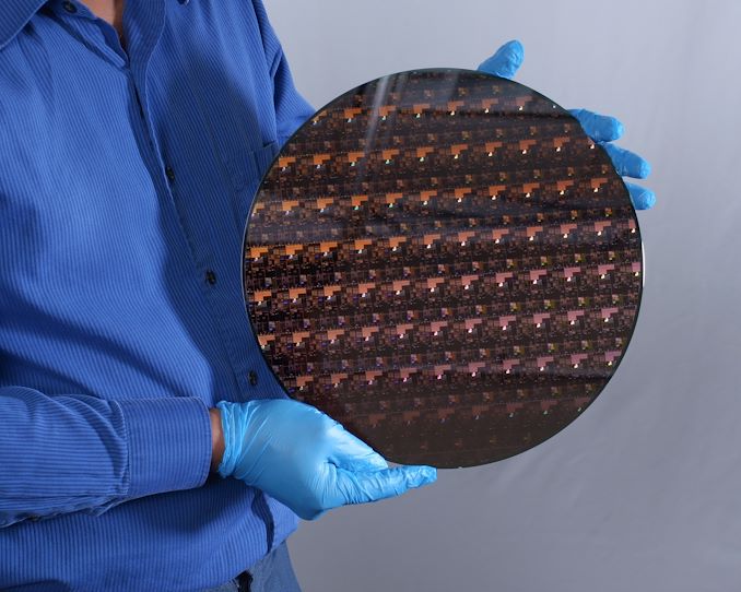
Every decade is the decade that tests the limits of Moore’s Law, and this decade is no different. With the arrival of Extreme Ultra Violet (EUV) technology, the intricacies of multipatterning techniques developed on previous technology nodes can now be applied with the finer resolution that EUV provides. That, along with other more technical improvements, can lead to a decrease in transistor size, enabling the future of semiconductors. To that end, Today IBM is announcing it has created the world’s first 2 nanometer node chip.
Names for Nodes
Just to clarify here, while the process node is being called ‘2 nanometer’, nothing about transistor dimensions resembles a traditional expectation of what 2nm might be. In the past, the dimension used to be an equivalent metric for 2D feature size on the chip, such as 90nm, 65nm, and 40nm. However with the advent of 3D transistor design with FinFETs and others, the process node name is now an interpretation of an ‘equivalent 2D transistor’ design.
Some of the features on this chip are likely to be low single digits in actual nanometers, such as transistor fin leakage protection layers, but it’s important to note the disconnect in how process nodes are currently named. Often the argument pivots to transistor density as a more accurate metric, and this is something that IBM is sharing with us.
Transistor Density
Today’s announcement states that IBM’s 2nm development will improve performance by 45% at the same power, or 75% energy at the same performance, compared to modern 7nm processors. IBM is keen to point out that it was the first research institution to demonstrate 7nm in 2015 and 5nm in 2017, the latter of which upgraded from FinFETs to nanosheet technologies that allow for a greater customization of the voltage characteristics of individual transistors.
IBM states that the technology can fit ’50 billion transistors onto a chip the size of a fingernail’. We reached out to IBM to ask for clarification on what the size of a fingernail was, given that internally we were coming up with numbers from 50 square millimeters to 250 square millimeters. IBM’s press relations stated that a fingernail in this context is 150 square millimeters. That puts IBM’s transistor density at 333 million transistors per square millimeter (MTr/mm2).
For comparison:
| Peak Quoted Transistor Densities (MTr/mm2) | ||||
| AnandTech | IBM | TSMC | Intel | Samsung |
| 22nm | 16.50 | |||
| 16nm/14nm | 28.88 | 44.67 | 33.32 | |
| 10nm | 52.51 | 100.76 | 51.82 | |
| 7nm | 91.20 | 237.18* | 95.08 | |
| 5nm | 171.30 | |||
| 3nm | 292.21* | |||
| 2nm | 333.33 | |||
| Data from Wikichip, Different Fabs may have different counting methodologies * Estimated Logic Density |
||||
As you can tell, different foundries have different official names with a variety of densities. It’s worth noting that these density numbers are often listed as peak densities, for transistor libraries where die area is the peak concern, rather than frequency scaling – often the fastest parts of a processor are half as dense as these numbers due to power and thermal concerns.
Stacked GAA
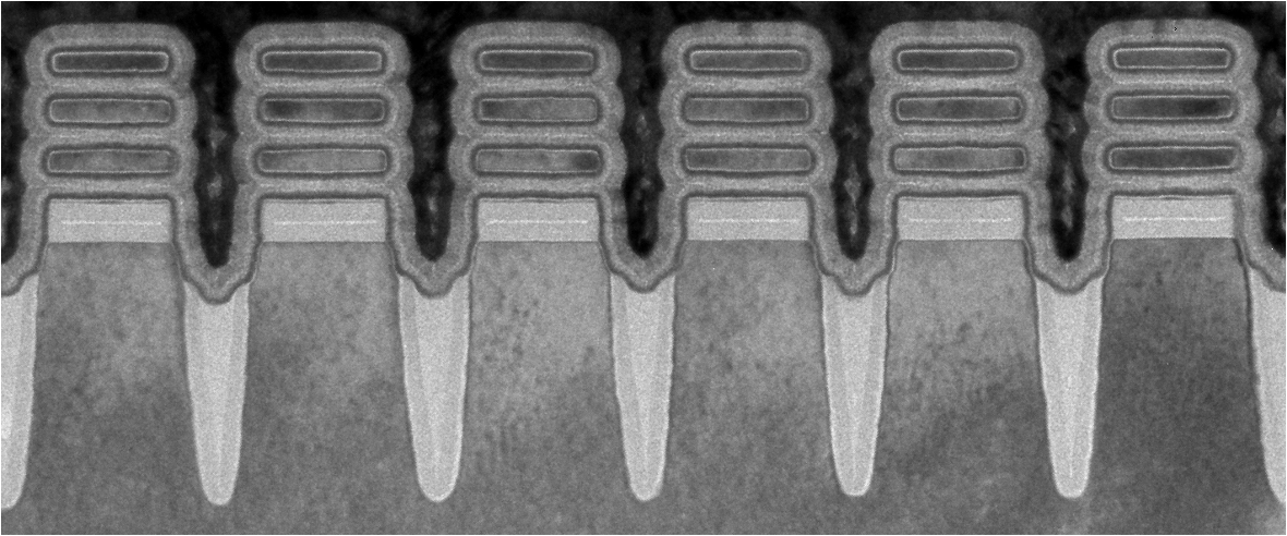
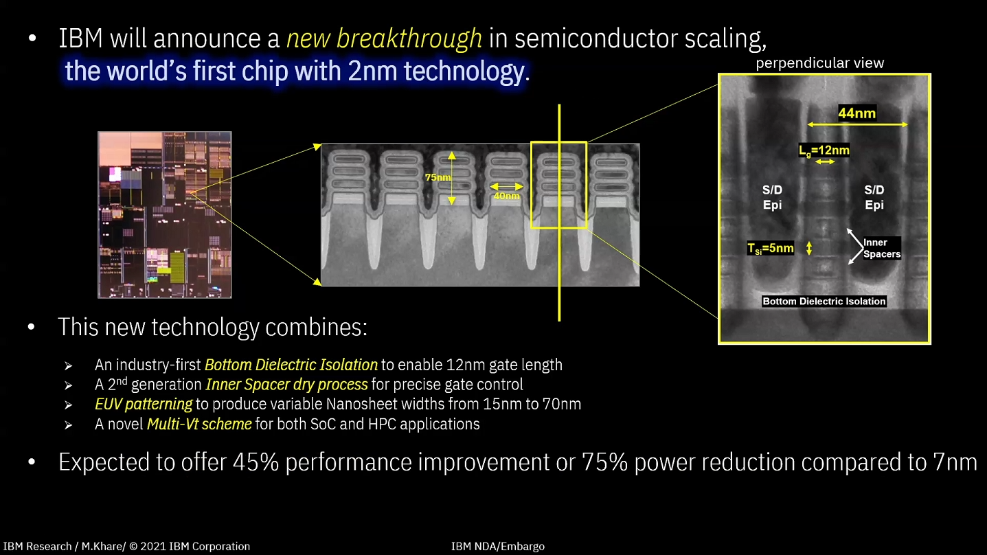
With regards the movement to Gate-All-Around / nanosheet transistors, while not explicitly stated by IBM, images show that this new 2nm processor is using a three-stack GAA design. Samsung is introducing GAA at 3nm, while TSMC is waiting until 2nm. Intel by contrast, we believe, will introduce some form of GAA on its 5nm process.
IBM’s 3-stack GAA uses a cell height of 75 nm, a cell width of 40 nm, and the individual nanosheets are 5nm in height, separated from each other by 5 nm. The gate poly pitch is 44nm, and the gate length is 12 nm. IBM says that its design is the first to use bottom dieletric isolation channels, which enables the 12 nm gate length, and that its inner spacers are a second generation dry process design that help enable nanosheet development. This is complimented by the first use of EUV patterning on the FEOL parts of the process, enabling EUV at all stages of the design for critical layers.
Users might be wondering why we’re hearing that IBM is the first to a 2nm chip. IBM is one of the world’s leading research centers on future semiconductor technology, and despite not having a foundry offering of their own, IBM develops IP in collaboration with others for their manufacturing facilities. IBM sold its manufacturing to GlobalFoundries with a 10 year partnership commitment back in 2014, and IBM also currently works with Samsung, and recently announced a partnership with Intel. No doubt the latter two will be partnering with IBM on some level around this new development for its viability in their own production chain.
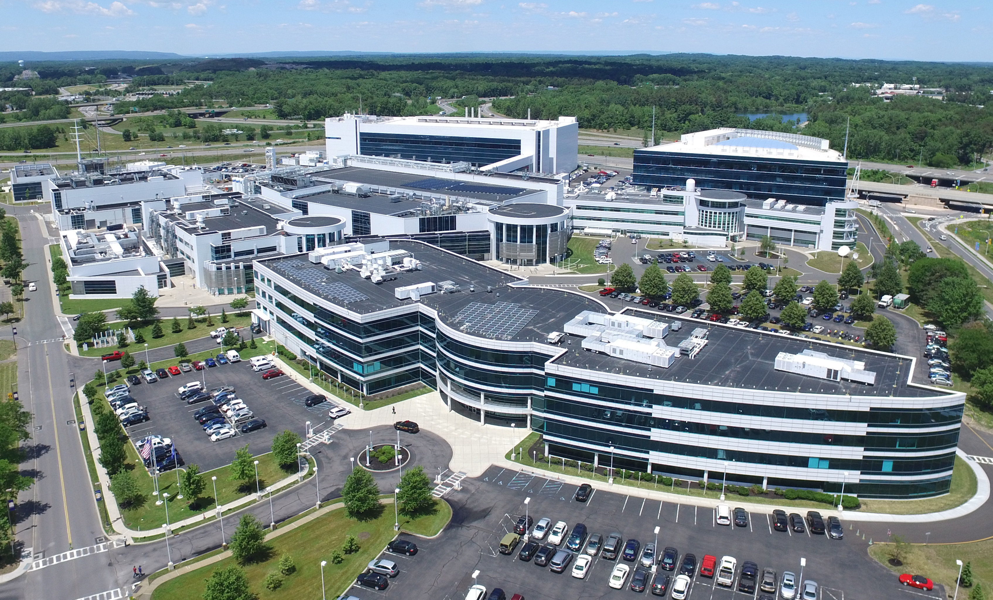
IBM Albany Research Center
No details on the 2nm test chip have been provided, although at this stage it is likely to be a simplified SRAM test vehicle with a little logic. The 12-inch wafer images showcase a variety of different light diffractions, which likely points to a variety of test cases to affirm the viability of the technology. IBM says that the test design uses a multi-Vt scheme for high-performance and high-efficiency application demonstrations.

Wafer up close
The chip was designed and made at IBM’s Albany research facility, which features a 100,000 sq. ft. clean room. The purpose of this facility is to build on IBM’s expansive patent and licensing portfolio for collaborations with partners.
We have a set of questions with IBM’s experts awaiting response. We also now have an active invitation to go visit, as and when we can travel again.
Related Reading
- IBM and AMD to Advance Confidential Computing
- Hot Chips 2020 Live Blog: IBM z15, a 5.2 GHz Mainframe CPU (11:00am PT)
- IBM & Partners to Fight COVID-19 with Supercomputers, Forms COVID-19 HPC Consortium
- Hot Chips 31 Live Blogs: IBM's Next Generation POWER
- IBM to use Samsung 7nm EUV for Next-Gen POWER and z CPUs
- IBM And Everspin Announce 19TB NVMe SSD With MRAM Write Cache
- TSMC Update: 2nm in Development, 3nm and 4nm on Track for 2022
- Intel’s Manufacturing Roadmap from 2019 to 2029: Back Porting, 7nm, 5nm, 3nm, 2nm, and 1.4 nm


118 Comments
View All Comments
Alistair - Thursday, May 6, 2021 - link
TSMC was not really that far ahead because of these differences in transistor densities, but now TSMC 5nm is close to where Intel is trying to get, but Intel is 3 years behind.Alistair - Thursday, May 6, 2021 - link
5nm is great, not surprised that Apple switched to Apple Silicon because of 5nm.Tams80 - Thursday, May 6, 2021 - link
It does suggest that most of the advantage Apple have gained over the competition has merely been from buying up all of another company's capacity than from their own work.But hey, an advantage is an advantage!
Otritus - Thursday, May 6, 2021 - link
Apple's IPC lead is generations ahead of the competition, and even if they were on 7nm the power efficiency loss would not be enough to eliminate their performance and efficiency lead. Also, Apple heavily invests in TSMC's new nodes, allowing them to partake as essentially beta testers for new nodes, so they aren't "buying up all of another company's capacity than from their own work" when they are investing in and working with the other company to get their leading architectures to perform well while transitioning the node from a beta release to a full release.michael2k - Thursday, May 6, 2021 - link
That's pretty false, especially if you read Anandtech:https://www.anandtech.com/show/16226/apple-silicon...
A14, which is the basis for the M1, has 8 wide decode, and as per Anandtech:
Featuring an 8-wide decode block, Apple’s Firestorm is by far the current widest commercialized design in the industry. IBM’s upcoming P10 Core in the POWER10 is the only other official design that’s expected to come to market with such a wide decoder design, following Samsung’s cancellation of their own M6 core which also was described as being design with such a wide design.
Other contemporary designs such as AMD’s Zen(1 through 3) and Intel’s µarch’s, x86 CPUs today still only feature a 4-wide decoder designs (Intel is 1+4) that is seemingly limited from going wider at this point in time due to the ISA’s inherent variable instruction length nature, making designing decoders that are able to deal with aspect of the architecture more difficult compared to the ARM ISA’s fixed-length instructions.
Fundamentally Apple's HW has been 8 wide since 2019, 7 wide since 2017, and besides that, features a huge re-order buffer and execution units:
A +-630 deep ROB is an immensely huge out-of-order window for Apple’s new core, as it vastly outclasses any other design in the industry. Intel’s Sunny Cove and Willow Cove cores are the second-most “deep” OOO designs out there with a 352 ROB structure, while AMD’s newest Zen3 core makes due with 256 entries, and recent Arm designs such as the Cortex-X1 feature a 224 structure.
On the Integer side, whose in-flight instructions and renaming physical register file capacity we estimate at around 354 entries, we find at least 7 execution ports for actual arithmetic operations. These include 4 simple ALUs capable of ADD instructions, 2 complex units which feature also MUL (multiply) capabilities, and what appears to be a dedicated integer division unit.
On the floating point and vector execution side of things, the new Firestorm cores are actually more impressive as they a 33% increase in capabilities, enabled by Apple’s addition of a fourth execution pipeline. The FP rename registers here seem to land at 384 entries, which is again comparatively massive. The four 128-bit NEON pipelines thus on paper match the current throughput capabilities of desktop cores from AMD and Intel, albeit with smaller vectors. Floating-point operations throughput here is 1:1 with the pipeline count, meaning Firestorm can do 4 FADDs and 4 FMULs per cycle with respectively 3 and 4 cycles latency. That’s quadruple the per-cycle throughput of Intel CPUs and previous AMD CPUs, and still double that of the recent Zen3, of course, still running at lower frequency.
So... process definitely means they can clock lower and consumer less power and pack more transistors in. However, even the 2018 A11 was fundamentally bigger in scope than AMD or Intel CPUs:
https://www.anandtech.com/show/13392/the-iphone-xs...
Monsoon (A11) and Vortex (A12) are extremely wide machines – with 6 integer execution pipelines among which two are complex units, two load/store units, two branch ports, and three FP/vector pipelines this gives an estimated 13 execution ports, far wider than Arm’s upcoming Cortex A76 and also wider than Samsung’s M3. In fact, assuming we're not looking at an atypical shared port situation, Apple’s microarchitecture seems to far surpass anything else in terms of width, including desktop CPUs.
kgardas - Thursday, May 6, 2021 - link
Basically every feature you praise is transistor invasive which means 5nm for apple is a need and is a huge advantage for them.Anyway, tremont is amd64 platform implementation and provide 2x 3-wide decoder while Intel noted that this may be combined in custom design into 1x 6-wide decoder. So 4-wide (5-wide Intel except Tremont) is just current implementations limitations on this platform and IIRC some Intel engineers already noted that they have much wider designs already done.
michael2k - Thursday, May 6, 2021 - link
Apple already had an 8 wide in 2019 with the A13 at 7nm:Apple’s microarchitecture being 8-wide actually isn’t new to the new A14. I had gone back to the A13 and it seems I had made a mistake in the tests as I had originally deemed it a 7-wide machine. Re-testing it recently, I confirmed that it was in that generation that Apple had upgraded from a 7-wide decode which had been present in the A11 and 12.
The big changes between A13 and A14 are additional 70 ROB and a 4th FP pipeline. So their 7nm process didn't give them any advantage over Intel's 10nm process (from this article 7nm TSMC only has a 91 MTr/mm2, vs 10nm Intel at 100 MTr/mm2), which means all performance can be attributed to Apple's 8 wide decode vs Intels' 4+1 wide decode, Apple's 560 ROB vs Intel's 352 ROB, Apple's 6 Int and 3 FP pipelines vs Intels combined 10 Int and FP pipelines (best as I can tell from Anandtech's 2019 Ice Lake review)
https://www.anandtech.com/show/14514/examining-int...
So... no, not unless you're arguing increasing the ROB from 560 to 630 and adding a 4th FP pipeline are transistor intensive.
Spunjji - Friday, May 7, 2021 - link
@michael2k one thing I always mentally note when I read these things is that Intel's 10nm density claim is from OG 10nm, not 10nm++SFROFL(etc.). I'm a little frustrated there hasn't been more of a detailed investigation into this from the tech press, because in practice even their low-performance designs like Lakefield seem to have a lower density than AMD's high-performance designs on TSMC 7nm.Spunjji - Friday, May 7, 2021 - link
Yes and no on that first sentence - Apple are definitely building designs that lean on transistor density, but at each respective node their designs have still been wider than competing x86 designs *on the same node*.name99 - Thursday, May 6, 2021 - link
"630 deep ROB"Like everything Apple has done, start by forgetting most of what you think you know...
Apple's ROB consists of ~330 "rows". A row has seven slots. "Generic" operations can go into any slot, but only one particular slot of the seven can hold "failable" operations (a branch or a load/store -- basically a thing that can mispredict and cause a flush).
So in principle you can pack the ROB with about 2300 NOPs (7*330).
In reality other constraints kick in earlier. The most significant is usually the history file, which has ~624 entries. (History file records every change to register mapping, and is used, along with the closest checkpoint, in rapid recovery from a mispredict).
But you can (I have tested this) create a pattern like (int op, fp op, store op) and pack 310 of these (ie 930 "real" ops) in the ROB. ie a reasonable claim for the size of the ROB is ~930, though use of loads (which fight with int and fp ops for history file space), will reduce this.
(For specialists, you will note that means 310 stores! How's that achieved? Surely not a 310 sized store queue? No, BUT non-speculative loads stores are subject to early completion and release!
The next obvious step -- early release of non-speculative registers -- is not present yet but Apple has a 2019 patent on this, and I wouldn't be surprised to see it in the A15.
You're still stuck with the HF limit, of course, but it would get you past the ~384+36 physical int and ~432 fp registers in dense int (common) and fp (less common) situations.
But Apple has so many register amplification techniques [the way movs are handled, the way immediates are handled, snarfing results off the bypass bus without register allocation for trivial cracked instructions] that physical register file limits are not that pressing -- and the design of Apple's physical register file is very very interesting giving you both that massive capacity and low power usage...)
The biggest constraint I see on "effective ROB size for most realistic code", going forward, is that History File limit, but I suspect that's actually easily fixed.
The real constraint is a "silent" one not visible in any structure -- it doesn't make sense to have a ROB larger than the distance over which you can effectively predict (both branches and load/store aliasing).
If I were a designer at Apple, that's how I would analyze the situation -- something needs to be done about the (rare, say one in a few hundred or so) hard-to-impossible to predict branches that essentially form a speculation barrier. Possibilities include
- predicating code past such instructions (easy'ish if there are just a few such instructions before the convergence point) or
- splitting into two execution streams at those rare but difficult branches. (micro-architecturally this looks much like SMT, only without visible OS/developer control; it's not an OS feature it's a hidden performance feature like branch prediction)