Update: PCI Express 6.0 Draft 0.71 Released, Final Release by End of Year
by Ryan Smith on July 2, 2021 7:00 AM EST- Posted in
- CPUs
- Interconnect
- PCIe
- PCI-SIG
- PCIe 6.0
Update 07/02: Albeit a couple of days later than expected, the PCI-SIG has announced this morning that the PCI Express draft 0.71 specification has been released for member review. Following a minimum 30 day review process, the group will be able to publish the draft 0.9 version of the specficiation, putting them on schedule to release the final version of the spec this year.
Originally Published 05/25
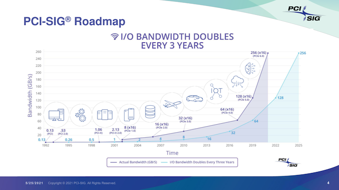
As part of their yearly developer conference, the PCI Special Interest Group (PCI-SIG) also held their annual press briefing today, offering an update on the state of the organization and its standards. The star of the show, of course, was PCI Express 6.0, the upcoming update to the bus standard that will once again double its data transfer rate. PCI-SIG has been working on PCIe 6.0 for a couple of years now, and in a brief update, confirmed that the group remains on track to release the final version of the specification by the end of this year.
The most recent draft version of the specification, 0.7, was released back in November. Since then, PCI-SIG has remained at work collecting feedback from its members, and is gearing up to release another draft update next month. That draft will incorporate the all of the new protocol and electrical updates that have been approved for the spec since 0.7.
In a bit of a departure from the usual workflow for the group, however, this upcoming draft will be 0.71, meaning that PCIe 6.0 will be remaining at draft 0.7x status for a little while longer. The substance of this decision being that the group is essentially going to hold for another round of review and testing before finally clearing the spec to move on to the next major draft. Overall, the group’s rules call for a 30-day review period for the 0.71 draft, after which the group will be able to release the final draft 0.9 specification.
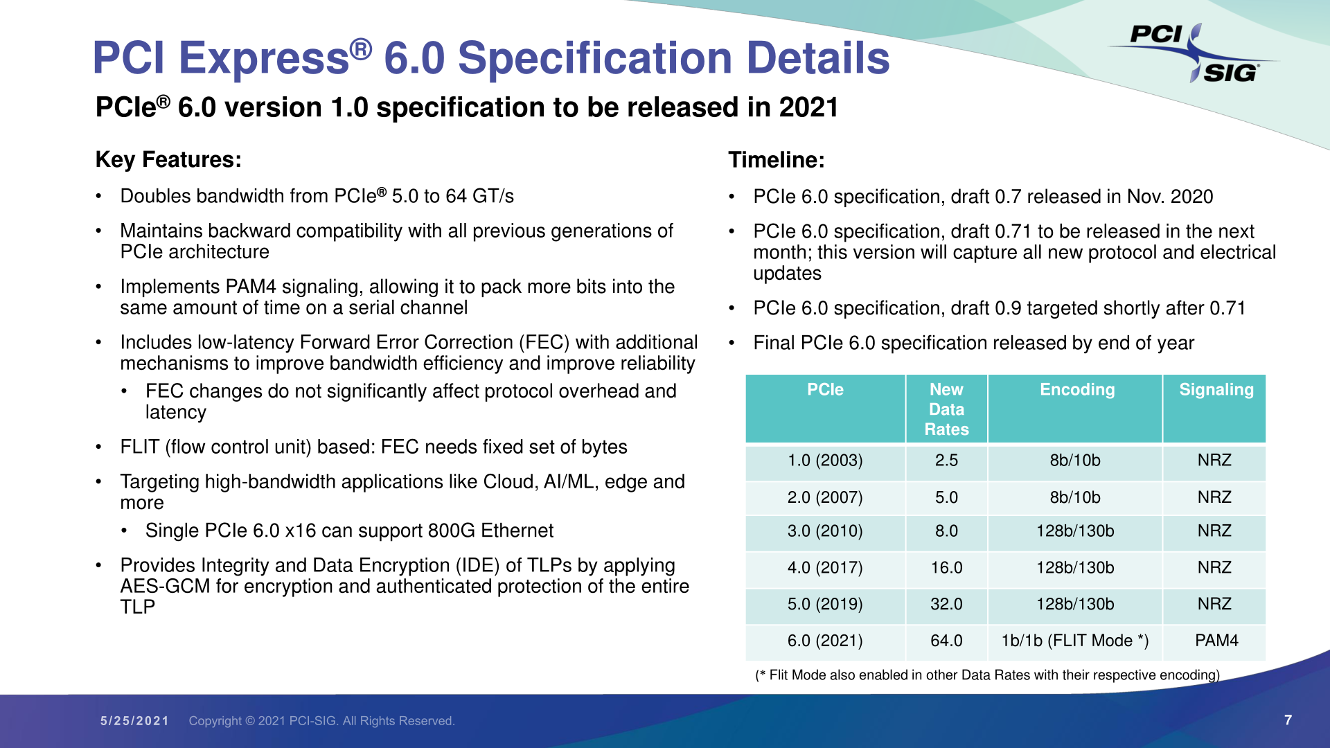
Ultimately, all of this is to say that PCIe 6.0 remains on track for its previously-scheduled 2021 release. After draft 0.9 lands, there will be a further two-month review for any final issues (primarily legal), and, assuming the standard clears that check, PCI-SIG will be able to issue the final, 1.0 version of the PCIe 6.0 specification.
In the interim, the 0.9 specification is likely to be the most interesting from a technical perspective. Once the updated electrical and protocol specs are approved, the group will be able to give some clearer guidance on the signal integrity requirements for PCIe 6.0. All told we’re not expecting much different from 5.0 (in other words, only a slot or two on most consumer motherboards), but as each successive generation ratchets up the signaling rate, the signal integrity requirements have tightened.
Overall, the unabashedly nerdy standards group is excited about the 6.0 standard, comparing it in significance to the big jump from PCIe 2.0 to PCIe 3.0. Besides proving that they’re once again able to double the bandwidth of the ubiquitous bus, it will mean that they’ve been able to keep to their goal of a three-year cadence. Meanwhile, as the PCIe 6.0 specification reaches completion, we should finally begin seeing the first PCIe 5.0 devices show up in the enterprise market.


103 Comments
View All Comments
mode_13h - Monday, July 5, 2021 - link
> amd could just do the same, use pcie 5 for the cpu to chipset link,> and leave everything else as 4, for check box parity.
If they know, for sure, that's what Intel is doing.
They might have been planning to design AM5 for PCIe 4.0, only. Intel's noise about PCIe 5 could have caused AMD to second guess themselves, and add in support for PCIe 5. That could cause delays and increased costs (due to more pins & larger footprint, if nothing else).
Tomatotech - Sunday, July 4, 2021 - link
Thanks for the July 2021 update!If PCIe 6.0 is approaching finalisation, that must mean work is starting on PCIe 7.0? Any rumours about the direction it will take? Do we have a date yet for the initial 0.3 draft?
mode_13h - Monday, July 5, 2021 - link
I wonder if they could do like a 4.1 that runs at PCIe 4.0's clock speed, but uses PAM4 to deliver PCIe 5.0 bandwidth. I wonder if that would be cheaper (or more power-efficient) to implement on desktops & laptops than PCIe 5.Tomatotech - Tuesday, July 6, 2021 - link
History is littered with the graves of many half-assed technology - and many fully-assed techs. I’m sorry that sounds like a half-assed short term effort that won’t go mainstream.mode_13h - Wednesday, July 7, 2021 - link
Thanks for sharing your opinion. I can think of less insulting ways to reject my suggestion.mode_13h - Wednesday, July 7, 2021 - link
And the problem it solves isn't only short-term. The signal integrity requirements of PCIe 5 aren't going to relax with time. And that means they're always going to add costs to PCIe 5.0 boards vs. PCIe 4.0.back2future - Tuesday, July 6, 2021 - link
Does "Remaining System Base Board Budget" still provide enough margin for PCIe sockets for full device-to-device bandwidth compared to NVlink 2.0/3.0 (so for PCIe 5.0 for about (36 minus 2*(9.5 plus 1.5) minus (4-7 pcb copper safety margin)) remaining 9-12dB for burst data transfer states on ~4 GB/s per lane and direction)?While NVlink switches are especially designed for that purpose (up to now 25-50Gbit/s, while PCIe 5.0 is standardized to 32GT/s, means 16Ghz maximum clock rate for data for error correction, header data and precoding/decoding? also on (NRZ) signaling scheme for 128b/130b coding scheme). Physical limitations for NVlink show real 90-95% of standardized bandwidth, sample is ~35Gbit/s for 40Gbit/s link (2 sub-lanes uplink to P100 NV-Pascal GPU).
PCISIG tells like this "The signal attenuation caused by the channel insertion loss (IL) is the biggest challenge of PCIe 5.0 technology system design.", what is recognized on about halfing maximum line length with doubling clock rates (>PCIe 3.x).
Comparison of expectations/potential for PCIe 5.0 and NVlink 2.0/3.0 would be pretty useful and readworthy (especially PCIe device-to-device rates for AI accelerators and databases/inference models storage)
back2future - Tuesday, July 6, 2021 - link
correction: remaining 7-10dB (on previous assumptions) on burst data transfer statesmode_13h - Wednesday, July 7, 2021 - link
I don't get your point about device-to-device. PCIe is a switched network, not a bus.back2future - Wednesday, July 7, 2021 - link
(PCI was a bus.) PCIe connects devices point to point and can support DMA for devices without affecting other PCIe connections (or devices) within a switch (or maybe the root package == chipset?). Seems there is no protocol overhead for "DMA"? accesses over switches, but for CPU/SoC connections for directly connected PCIe devices (hardware managed?) this might differ?NVlink is called a bus system and NVlink bridge (for example) is a parallel bandwidth path additional to PCIe and data transfer is managed on each graphic card's NVlink controller? This changes on a NVlink switch that connects through 6-12 (V100-A100) switching interfaces up to 8-16 graphic devices (point to point through the switch)?
Maybe it is fair enough to summarize, that switches (for PCIe, NVlink) can connect devices like these were on physically paralleled lanes if suitable for "DMA"?