Intel Architecture Day 2021: Alder Lake, Golden Cove, and Gracemont Detailed
by Dr. Ian Cutress & Andrei Frumusanu on August 19, 2021 9:00 AM EST
This week Intel held its annual Architecture Day event for select press and partners. As with previous iterations, the company disclosed details about its next generation architectures set to come to the market over the next twelve months. Intel has promised the release of its next-generation consumer and mobile processor family, Alder Lake, to come by the end of the year and today the company is sharing a good number of details about the holistic design of the chips as well as some good detail about the microarchitectures that form this hybrid design: Golden Cove and Gracemont. Here is our analysis of Intel’s disclosure.
Alder Lake: Intel 12th Gen Core
As mentioned in previous announcements, Intel will launch its Alder Lake family of processors into both desktop and mobile platforms under the name of Intel’s 12th Gen Core Processors with Hybrid Technology later this year. This is Intel’s second generation hybrid architecture built on Intel 7 process node technology. The hybrid design follows Intel Lakefield designs for small notebooks launched last year. The nature of a hybrid design in Intel nomenclature involves having a series of high ‘Performance’ cores paired with a number of high ‘Efficiency’ cores. Intel has simplified this into P-core and E-core terminology.
For Alder Lake, the processor designs feature Performance cores based on a new Golden Cove microarchitecture, and Efficiency cores based on a new Gracemont architecture. We will cover both over the course of this article, however the idea is that the P-core is preferential for single threaded tasks that require low latency, and the E-core is better in power limited or multi-threaded scenarios. Each Alder Lake SoC will physically contain both, however Intel has not yet disclosed the end-user product configurations.
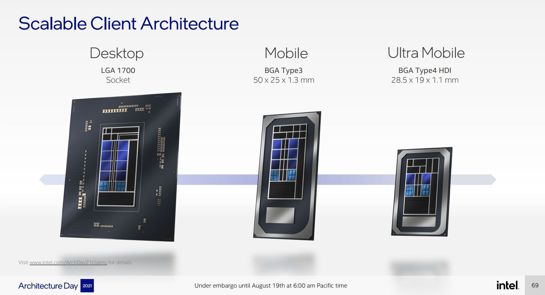
Each of the P-cores has the potential to offer multithreading, whereas the E-cores are one thread per core. This means there will be three physical designs based on Alder Lake:
- 8 P-core + 8 E-core (8C8c/24T) for desktop on a new LGA1700 socket
- 6 P-core + 8 E-core (6C8c/20T) for mobile UP3 designs
- 2 P-core + 8 E-core (2C8c/12T) for mobile UP4 designs
Intel typically highlights UP4 mobile designs for very low power installs, down to 9 W, whereas UP3 can cover anything from 12 W to 35 W (or perhaps higher), but when asked about the power budgets for these processors, Intel stated that more detail will follow when product announcements are made. Intel did confirm that the highest client power, presumably on the desktop processor, will be 125 W.
Highlighted in our discussions is how modular Intel has made Alder Lake. From a range of base component options, the company mixed and matched what it felt were the best combination of parts for each market.
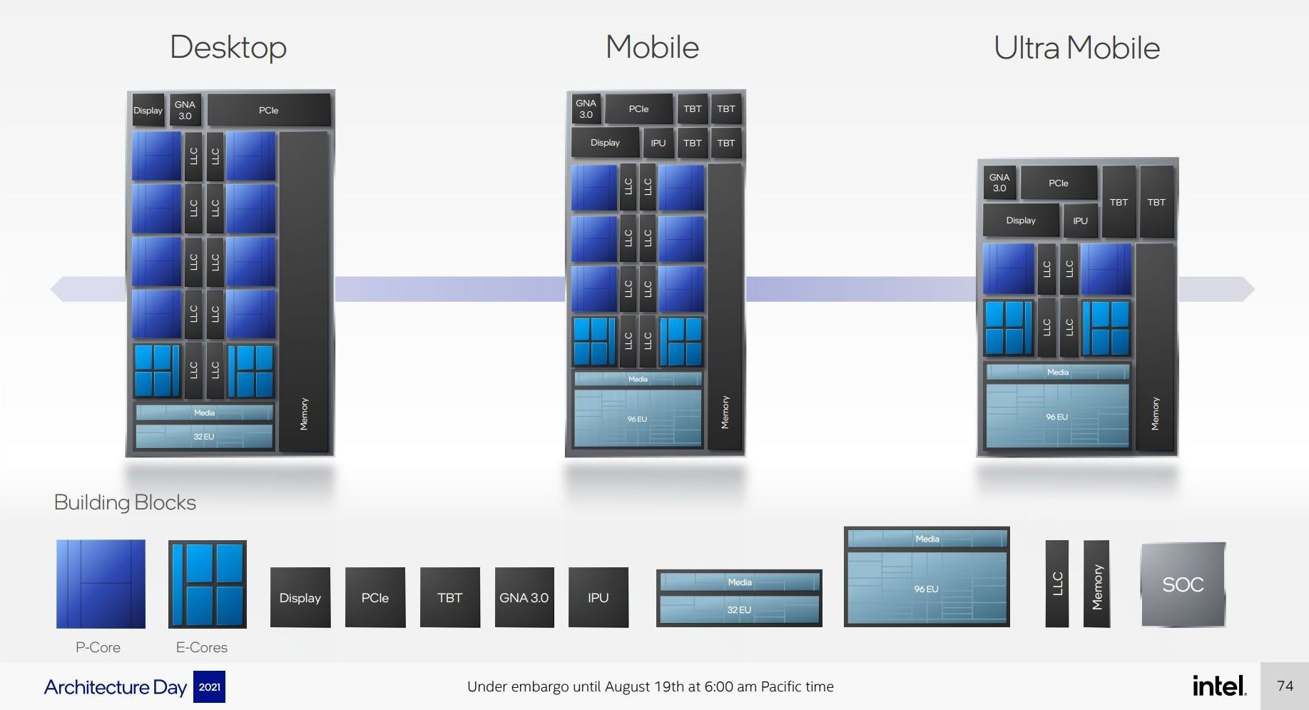
Here it shows that four E-cores takes up the same physical space as one P-core, but also that the desktop hardware will at most have 32 EUs (Execution Units) for Xe-LP graphics (same as the previous generation), while both of the mobile processors will offer 96 physical EUs that may be disabled down based on the specific line item in the product stack.
All three processors will feature Intel’s next generation Gaussian Neural Accelerator (GNA 3.0) for minor low power AI tasks, a display engine, and some level of PCIe, however the desktop processor will have more. Only the mobile processors will get an Image Processing Unit (IPU), and Thunderbolt 4 (TBT), and here the big UP3 mobile processor gets four ports of Thunderbolt whereas the smaller UP4 will only get two. The desktop processor will not have any native Thunderbolt connectivity.
A bit more info on the Desktop Processor IO and Interconnect
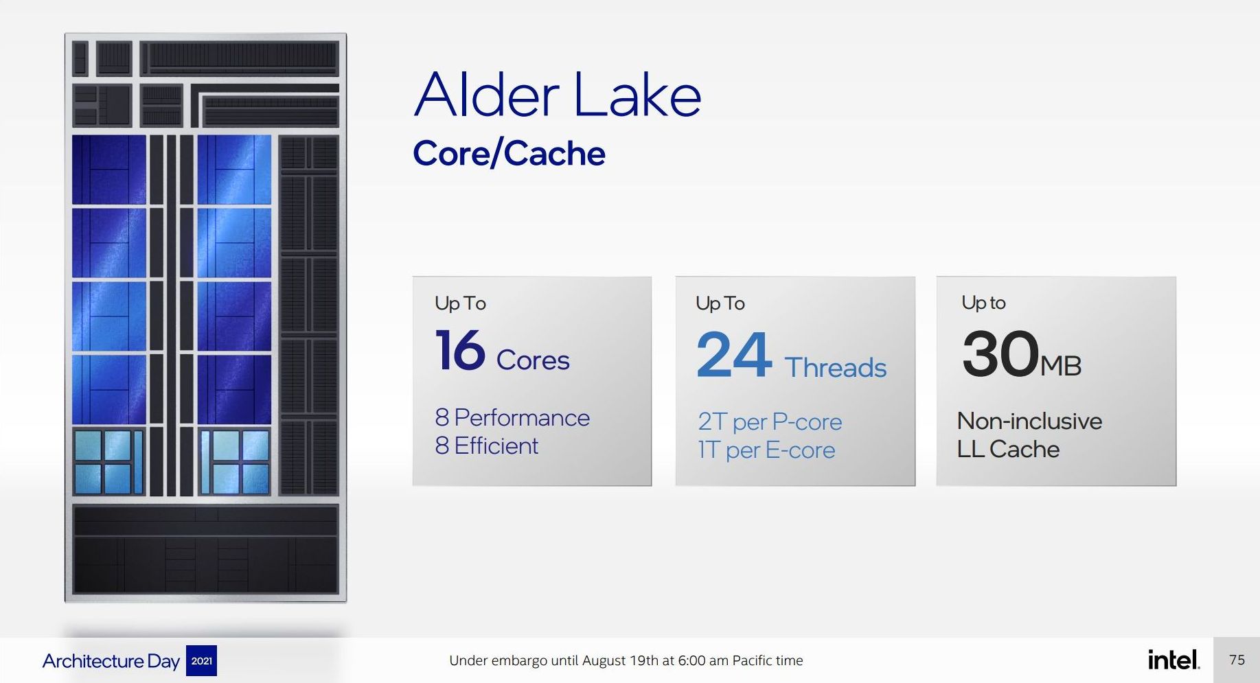
We’ll cover a bit more detail about the core designs later in this article, but Intel did showcase some of the information on the desktop processor. It confirmed explicitly that there would be 16 total cores and 24 threads, with up to 30 MB of non-inclusive last level/L3 cache.
In contrast to previous iterations of Intel’s processors, the desktop processor will support all modern standards: DDR5 at 4800 MT/s, DDR4-3200, LPDDR5-5200, and LPDDR4X-4266. Alongside this the processor will enable dynamic voltage-frequency scaling (aka turbo) and offer enhanced overclocking support. What exactly that last element means we’re unclear of at this point.
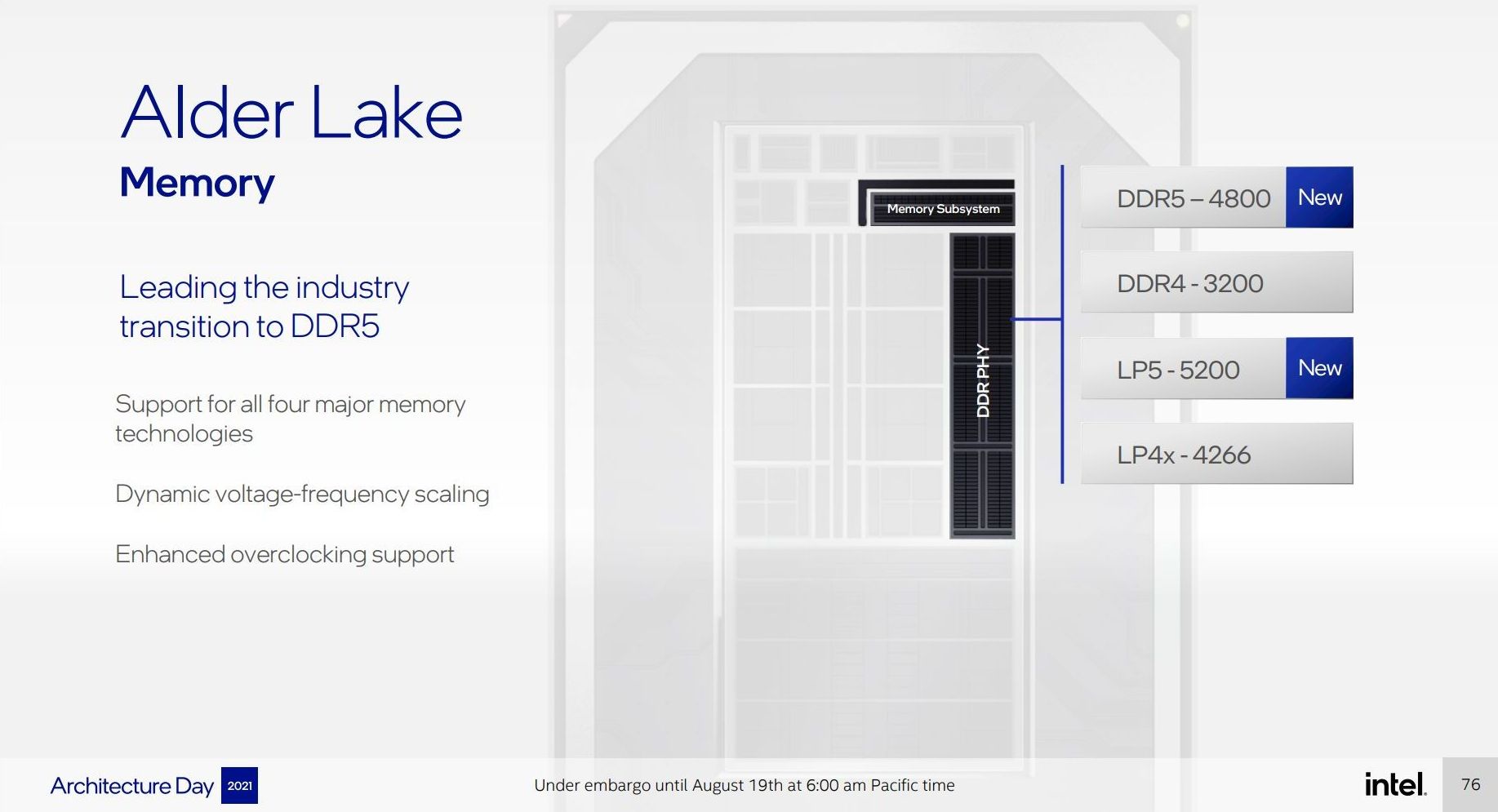
Intel confirmed that there will not be separate core designs with different memory support – all desktop processors will have a memory controller that can do all four standards. What this means is that we may see motherboards with built-in LPDDR5 or LPDDR4X rather than memory slots if a vendor wants to use LP memory, mostly likely in integrated small form factor designs but I wouldn’t put it past someone like ASRock to offer a mini-ITX board with built in LPDDR5. It was not disclosed what memory architectures the mobile processors will support, although we do expect almost identical support.
On the PCIe side of things, Alder Lake’s desktop processor will be supporting 20 lanes of PCIe, and this is split between PCIe 4.0 and PCIe 5.0.
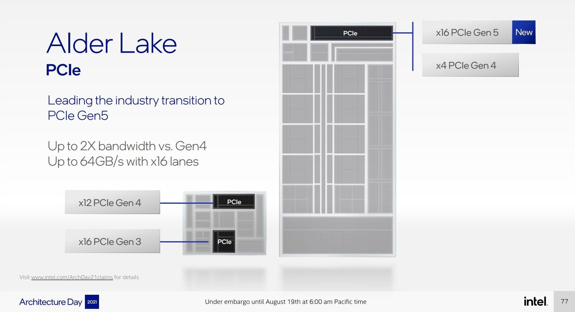
The desktop processor will have sixteen lanes of PCIe 5.0, which we expect to be split as x16 for graphics or as x8 for graphics and x4/x4 for storage. This will enable a full 64 GB/s bandwidth. Above and beyond this are another four PCIe 4.0 lanes for more storage. As PCIe 5.0 NVMe drives come to market, users may have to decide if they want the full PCIe 5.0 to the discrete graphics card or not
Intel also let it be known that the top chipset for Alder Lake on desktop now supports 12 lanes of PCIe 4.0 and 16 lanes of PCIe 3.0. This will allow for additional PCIe 4.0 devices to use the chipset, reducing the number of lanes needed for items like 10 gigabit Ethernet controllers or anything a bit spicier. If you ever thought your RGB controller could use more bandwidth, Intel is only happy to provide.
Intel did not disclose the bandwidth connectivity between the CPU and the chipset, though we believe this to be at least PCIe 4.0 x4 equivalent, if not higher.
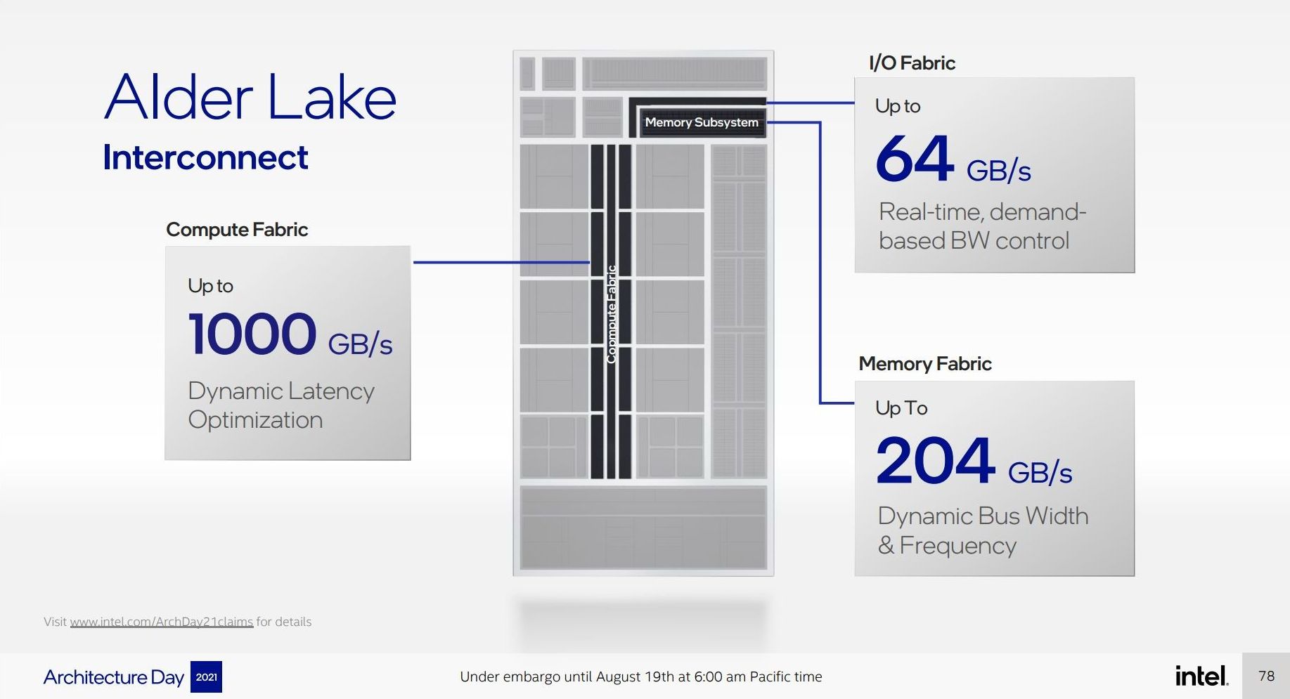
The Alder Lake processor retains the dual-bandwidth ring we saw implemented in Tiger Lake, enabling 1000 GB/s of bandwidth. We learned from asking Intel in our Q&A that this ring is fully enabled regardless of whether the P-cores or E-cores are being used – Intel can disable one of the two rings when less bandwidth is needed, which would save power, however based on previous testing this single ring could end up drawing substantial power compared to the E-cores in low power operation. (This may be true in the mobile processors as well, which would have knock on effects for mobile battery life.)
The 64 GB/s of IO fabric is in line with the PCIe 5.0 x16 numbers we saw above, however the 204 GB/s of memory fabric bandwidth is a confusing number. Alder Lake features a 128-bit memory bus, which allows for 4x 32-bit DDR5 channels (DDR5 has two 32-bit channels per module, so 2 modules still), however in order to reach 204 GB/s in that configuration requires DDR5-12750; Intel has rated the processor only at DDR5-4800, less than half that, so it is unclear where this 204 GB/s number comes from. For perspective, Intel’s Ice Lake does 204.8 GB/s, and that’s a high-power server platform with 8 channels of DDR4-3200.
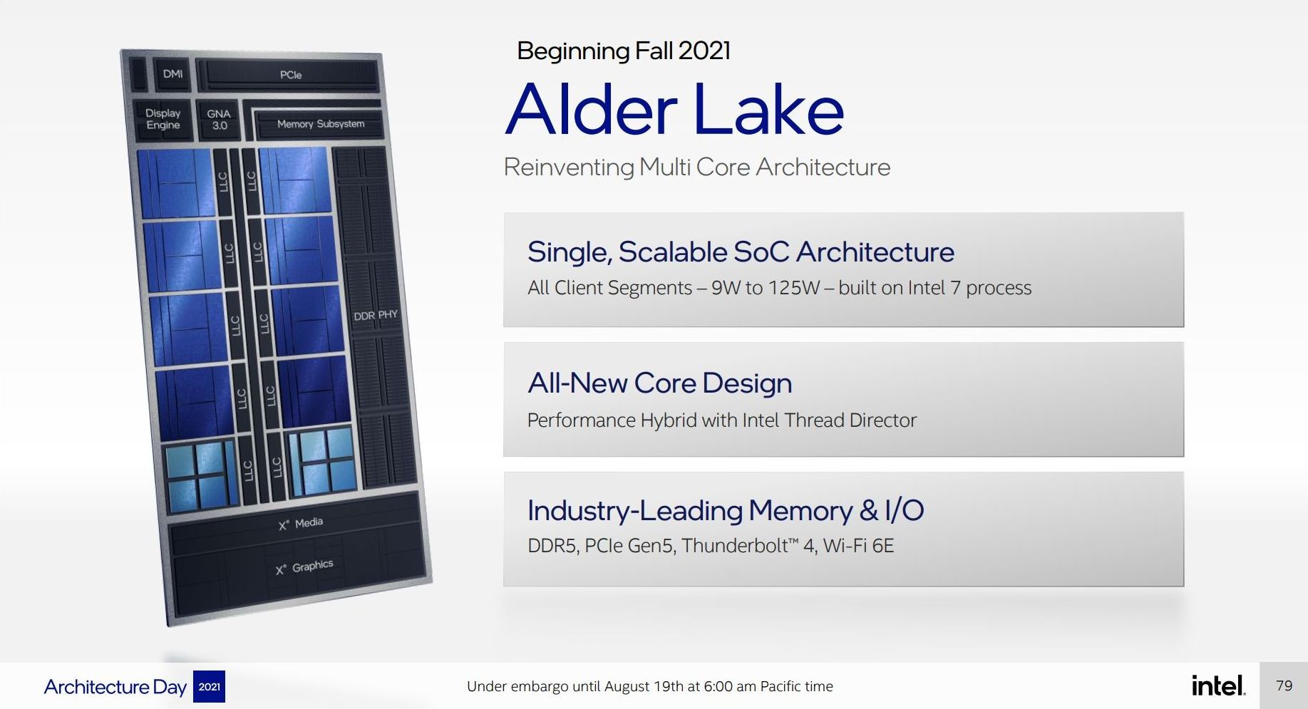
This final slide mentions TB4 and Wi-Fi 6E, however as with previous desktop processors, these are derived from controllers attached to the chipset, and not in the silicon itself. The mobile processors will have TBT integrated, but the desktop processor does not.
This slide also mentions Intel Thread Director, which we want to address on the next page before we get to the microarchitecture analysis.


223 Comments
View All Comments
name99 - Thursday, August 19, 2021 - link
"Intel’s Thread Director controller puts an embedded microcontroller inside the processor such that it can monitor what each thread is doing and what it needs out of its performance metrics. It will look at the ratio of loads, stores, branches, average memory access times, patterns, and types of instructions."People might be interested to know that Apple has done this for years (I don't know about ARM).
The Apple scheme has many moving parts but these include
- tracking how much work is done by Fetch, Decode and Execute. The first two can estimate based on number of instructions, the third takes account of the type of instruction.
- the scheme is even sophisticated enough (at least the patent talks about this) that the weights given to each of these pieces are variable to match the characteristics of the manufactured chip. Each SoC is tested and the precise weights are fused into the chip after testing.
- this mean that the SoC can calculate things like instantaneous power usage. This is used at the overall SoC level (to limit battery current draw) and at the per execution unit level (eg to halt the SIMD pipeline for a cycle every few cycles if some thermal pr power constraint is being exceeded). You will notice this is the equivalent of Intel's frequency throttling for AVX512, but much nicer because it is done on demand, purely to the level needed, and without slowing down the rest of the core or without a slow transition between faster and slower frequencies.
- there is also tracking of where L1 cache fills comes from. If a lot come from the E cores, the E-core frequency is boosted. If a lot come from DRAM, then the fabric frequency and DRAM frequency are boosted.
- behind everything, for *most purposes* the primary metric is nJ/instruction. The scheduler does many things in the obvious way you would expect (background threads on E cores, track progress vs deadline and ramp core performance up or down depending on how that is doing); but some non-obvious things are that code that is inefficient (ie nJ/instruction is too low) and that is not otherwise protected by the OS will be pushed to lower frequency or to an E-core. This might sound bad, but mainly what it's saying is
+ if you're constantly waiting on DRAM, then running the core at high frequency does you no good anyway
+ if you're not running very wide (hard to predict branches, or long dependency chains) you can't take advantage of the big core anyway, so why waste power keeping you there?
Presumably Intel's scheme at least covers all these sorts of bases.
One complication Apple has, that I assume Intel/Windows will not have (but it's not clear) is the use of clustering. Clustering sounds great, as does that huge low latency shared cache. But it comes at the cost of, as far as I can tell, a common frequency for the entire cluster. (If CPUs were at different frequencies, there'd have to be a cross-frequency-domain stage when communicating with the shared L2, at that would add noticeable latency).
So the OS scheduler doesn't just have the job of scheduling each thread to the optimal core at optimal DVFS, it also has to pack 4 optimal [as a unit] threads to a cluster...
I can't tell if Intel's scheme runs their small cores that way, as a cluster of 4 sharing an L2 (and thus sharing frequency). If so, how the OS scheduler handles this is something to keep an eye on for both Windows and Linux.
BTW there are very recently published patents that suggest Apple may be moving away from this, to a scheme of private L2s and a shared per-cluster L3!
https://patents.google.com/patent/US10942850B2
That's something to keep an eye on for the A15 and M2...
mode_13h - Friday, August 20, 2021 - link
Thanks for the info.What do you mean by "nJ/instruction" ? Is that the ratio of branches vs. non-branch instructions? If not, then what does it have to do with DRAM latency? Or was that a reference to the prior paragraph?
Where do you read this stuff?
name99 - Friday, August 20, 2021 - link
nanoJoules/instruction. ie energy per instructionThis info is acquired from reading massive numbers of Apple patents, validated as much as possible by experiments run on M1.
mode_13h - Saturday, August 21, 2021 - link
Wow. My eyes glaze over, trying to read patents. I'm sure there are better and worse ones, but they're often written in ways that drain the joy out of the most interesting ideas.Thanks for sharing!
jospoortvliet - Sunday, August 22, 2021 - link
Indeed super interesting!mode_13h - Thursday, August 19, 2021 - link
I wonder if they did anything to the decoder around SMT or multiple instruction streams. In Tremont, it seemed like they way they used a 6-wide decoder was as two 3-wide decoders, where each would work on a separate branch target.> the L2 BTB (branch target buffer) has grown to well over double with the
> structure increased from 5K entries to 12K entries
Can someone refresh us on the function of a BTB? Is it like a cache that stores the target address of each recent branch instruction, so that speculative execution doesn't have to wait for the target to be computed (if not a fixed target)?
> actually eliminating instructions that otherwise would have to actually
> emitted to the back-end execution resources.
Huh? Seems like an editing error. Can anyone elaborate?
> Intel still continues to use merged execution port / reservation station design
Someone please remind us what a reservation station is?
> On the integer side of things, there’s now a fifth execution port and pipeline with
> simple ALU and LEA capabilities
In this case, I presume LEA means "load effective address" and is used to compute memory addresses (potentially involving a multiply, an add, a constant offset?). Is that correct? And does the above statement mean that each of those ports can do simple ALU *or* LEA operations?
> Intel has improved the prefetchers
Yes, and the article text didn't even mention the bullet point in the slide about feedback-based prefetch-throttling! I'm reminded of how ARM's N2 can throttle back prefetching, during periods of memory contention. Perhaps Intel came to the same conclusion that overzealous prefetchers can starve cores running memory-intensive routines, in highly-threaded workloads.
> full-line-write predictive bandwidth optimisation ... where the core can greatly improve
> bandwidth by avoiding RFO reads of cache lines that are going to be fully rewritten
Yes, I've been wanting this for about 2 decades.
> We can see in the graph ... low outliers where the new design doesn’t improve thing
> much or even sees regressions, which is odd.
Maybe those were affected by the disabling of AVX-512? Or were those benchmarks performed on a fully-enabled core?
> +25% wider µOP output
If this is referring to expanding uOP cache outputs from 6 -> 8, that's a 33% improvement!
name99 - Thursday, August 19, 2021 - link
"Can someone refresh us on the function of a BTB? "It's hard to be sure because I can never tell the extent to which Intel is doing things the old comfortable way, or the most sensible new way. I'll tell you what Apple do.
Intel are presumably a subset of these features, but I don't know how good a subset. You need ALL the pieces to run sustained "random" code 8-wide as Apple does.
(a) You want a predictor for indirect branches (think things like virtual function or procPtr calls). How to construct such a predictor is interesting but we will just assume it exists. This may have been what the original Branch Target Buffer was say in the early 1990s, but it is NOT what we have in mind today.
(b) To run a modern wide OoO machine optimally, you want to be able to process a TAKEN branch per cycle. (Code has a branch every ~6 instructions, a taken branch every ~10 instructions. If you want to run 8 wide...)
- This means you need to pull a new run of instructions (ie loaded from a new address) every cycle.
- This, in turn, means that you really need to run Fetch as an asynchronous process. A Fetch Engine every cycle predicts the next Fetch Address and the number of instructions to Fetch. (On Apple this can be at least as wide as 16 instructions in one cycle if everything lines up correctly.) These instructions are placed in the Fetch Queue and at the other end Decode reads 8/cycle from this queue. Making Fetch async from the rest of the machine means that you can sometimes pull in 16 instructions into the queue, sometimes you just pull in three or four instructions, sometimes none while you wait for a cache miss. But hopefully the queue between Fetch and Decode buffers much of this variation.
- BUT asynchronous Fetch means Fetch is on its own regarding how it proceeds. Basically what you want is
+ a very fast (single cycle!) Next Fetch Predictor that produces the next fetch address and (ideally) also a Fetch Width
But a fast such predictor is of limited accuracy.
So the second essential you need is very high quality predictors that correct the Next Fetch Predictor. As long as you correct a misFetch before the instruction stream hits Rename life is fairly easy. Correcting after Rename is tough (you have to undo resource allocations), correcting after Issue is hopeless and you have to flush.
The Apple numbers are that their high quality predictors (Branch Prediction and Indirect Branch Prediction) are TAGE based, phenomenally accurate, and take up to 5 cycles to generate a result. That just works out (of course!)
So the idea is that the Next Fetch Predictor generates a stream of Fetch's which results in a stream of, let's call them cars of instructions, proceeding from I-cache, through the Fetch Queue, through Decode. At any point one of the better quality predictors can step in and derail all the cars after a certain point, so that Fetch restarts. Obviously this isn't great, you've lost up to five cycles of work, but it's a lot better than a full machine flush!
OK, within this framework, I believe that what Intel today calls the BTB is essentially doing the same job as what I am calling the Next Fetch Predictor.
BTW there are an insane number of tweaks and improvement Apple have made to the above scheme over the years. These include
- a separate Return stack used by the Next Fetch predictor to deal with extremely rapid call/return pairs (eg call, work, return is three cycles; all done before the code has even hit decode, so totally out of sync with the "full accuracy" Return stack)
- Decode (ie the earliest stage possible) does what it can to keep the machinery on track. Decode detects any sort of mismatch between decoded branches and the next car of instructions and, if so, gets Fetch to resteer. This is easily done for unconditional branches, and can also be done for a few other weird cases (like some mismatched call/return pairs). Decode also updates the Return stack.
- pre-decode (ie when an instruction line is moved from l2 to L1) does a bunch of stuff to mark significant points (eg where branches are) in a cache line. This in turn is referenced the first time the Next Fetch Predictor encounters these new lines.
- for certain cases (most obviously when the Next Fetch Predictor has an indirect branch marked as low confidence) Fetch pauses until some of the upstream machinery can suggest an address. The idea is that for low confidence indirect branches, you're so unlikely to guess correctly why even waste energy trying?
Apart from all these, theres a whole other set of machinery that handles loops and the transition from "random" code to loops. These include both an L0 cache and a trace cache. (That's right kids, a trace cache!)
There's also a whole set of ideas for saving power at every stage of this process. For example the Next Fetch Predictor, along with the obvious things it is recording (next fetch address, and fetch width) also records two items obvious in retrospect -- the physical address (so no TLB lookup necessary) and even the cache way (so no way prediction necessary, and the correct way -- and only that way) can be fired up on cache access. The loop buffer, L0, and the trace cache are additional ways to run Fetch on energy fumes for code that meets the specific requirements, so that various of TLB, way prediction, multi-way lookup, branch predictor, etc etc can all be powered down.
mode_13h - Friday, August 20, 2021 - link
Thanks for the info. I wonder where you find such detailed descriptions!> L0 cache
Just another name for a uop cache?
> That's right kids, a trace cache!
So, a trace cache stores an entire string of instructions, even across one or more branches? Does it hold instructions before or after decode?
> and even the cache way
You mean the cache set?
> The loop buffer
What's a loop buffer? Sort of like a trace cache, for loops?
name99 - Friday, August 20, 2021 - link
Think of the steps required to run normal code, as I described above. The consider various simple loops.Suppose you have a straight line loop, say 40 instructions in the loop body, no branches. Then you can omit branch prediction, TLB, cache -- just repeatedly run the same code from a straight buffer. That's essentially a loop buffer.
Now suppose that your loop body has a few branches in it, but they are predictable, maybe something like
if(loop counter even){path1} else {path2}
Now what you want is something like a trace cache that's holding the two paths path1 and path2, and a very simple predictor that's telling which of these to choose each iteration. You can still avoid the costs of a real branch predictor and a real cache.
Now suppose you have a loop with moderately complicated branches, not terrible but not that easy to predict either. You can't avoid the cost of branch prediction now (as I said, to validate the guess of the Next Fetch Predictor) but you can avoid much of the cost of the cache by moving the loop body into an L0 cache which will be essentially a small direct-mapped cache. Being smaller, and direct-mapped, it will use less energy/access than the full I-cache. (And you probably will also access it virtually rather than physically, so also avoid TLB costs.)
cache way:
Recall that a DIRECT-MAPPED cache has only a single place where a line can go -- grab some bits from the middle of an address, they define an index, the line goes at that index. This is fast and cheap, but means you have a problem if you frequently want to access two addresses with the same index (ie same middle bits in their addresses).
n-way set-associative cache means you now have, n (may be 2, 4, 8 or some other number) of slots associated with a given index. So if you have 8 slots, you can hold 8 lines with that same index, ie 8 addresses with those same middle bits.
BUT how do you know WHICH of those 8 lines you want? Ahh.
That gets into the business of matching tags, way prediction and a whole mess of other stuff that you need to read in a textbook. But the relevance to what I was saying is that which of these 8 possible lines is of interest is called a WAY. So by storing the cache way, you can access a cache with the speed (avoid cache tag lookup) and energy (no need to precharge the tags) of a direct-mapped cache.
GeoffreyA - Saturday, August 21, 2021 - link
Great information. I believe on the Intel side, Nehalem added something like that, the LSD.