Intel Architecture Day 2021: Alder Lake, Golden Cove, and Gracemont Detailed
by Dr. Ian Cutress & Andrei Frumusanu on August 19, 2021 9:00 AM EST
This week Intel held its annual Architecture Day event for select press and partners. As with previous iterations, the company disclosed details about its next generation architectures set to come to the market over the next twelve months. Intel has promised the release of its next-generation consumer and mobile processor family, Alder Lake, to come by the end of the year and today the company is sharing a good number of details about the holistic design of the chips as well as some good detail about the microarchitectures that form this hybrid design: Golden Cove and Gracemont. Here is our analysis of Intel’s disclosure.
Alder Lake: Intel 12th Gen Core
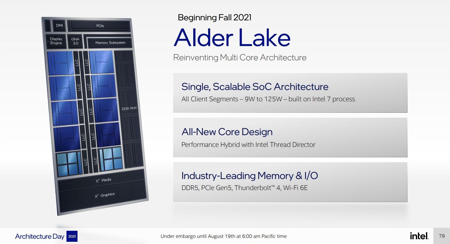
As mentioned in previous announcements, Intel will launch its Alder Lake family of processors into both desktop and mobile platforms under the name of Intel’s 12th Gen Core Processors with Hybrid Technology later this year. This is Intel’s second generation hybrid architecture built on Intel 7 process node technology. The hybrid design follows Intel Lakefield designs for small notebooks launched last year. The nature of a hybrid design in Intel nomenclature involves having a series of high ‘Performance’ cores paired with a number of high ‘Efficiency’ cores. Intel has simplified this into P-core and E-core terminology.
For Alder Lake, the processor designs feature Performance cores based on a new Golden Cove microarchitecture, and Efficiency cores based on a new Gracemont architecture. We will cover both over the course of this article, however the idea is that the P-core is preferential for single threaded tasks that require low latency, and the E-core is better in power limited or multi-threaded scenarios. Each Alder Lake SoC will physically contain both, however Intel has not yet disclosed the end-user product configurations.
Each of the P-cores has the potential to offer multithreading, whereas the E-cores are one thread per core. This means there will be three physical designs based on Alder Lake:
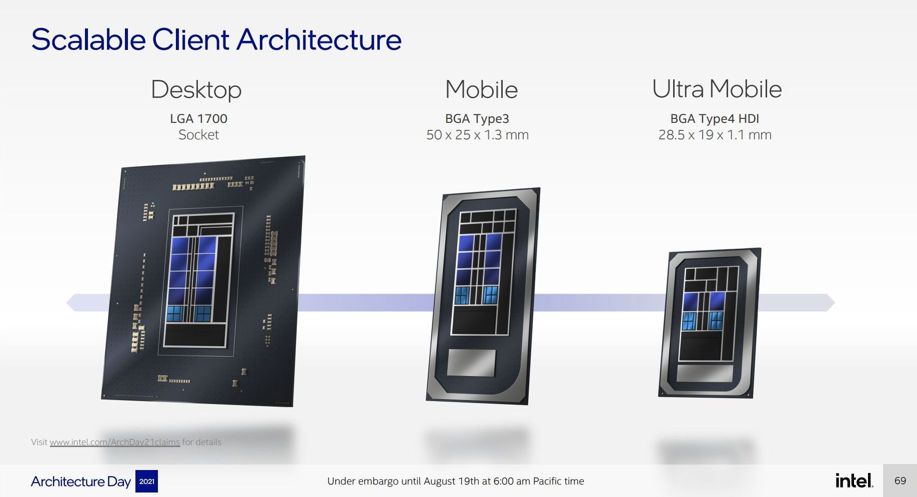
- 8 P-core + 8 E-core (8C8c/24T) for desktop on a new LGA1700 socket
- 6 P-core + 8 E-core (6C8c/20T) for mobile UP3 designs
- 2 P-core + 8 E-core (2C8c/12T) for mobile UP4 designs
Intel typically highlights UP4 mobile designs for very low power installs, down to 9 W, whereas UP3 can cover anything from 12 W to 35 W (or perhaps higher), but when asked about the power budgets for these processors, Intel stated that more detail will follow when product announcements are made. Intel did confirm that the highest client power, presumably on the desktop processor, will be 125 W.
Highlighted in our discussions is how modular Intel has made Alder Lake. From a range of base component options, the company mixed and matched what it felt were the best combination of parts for each market.
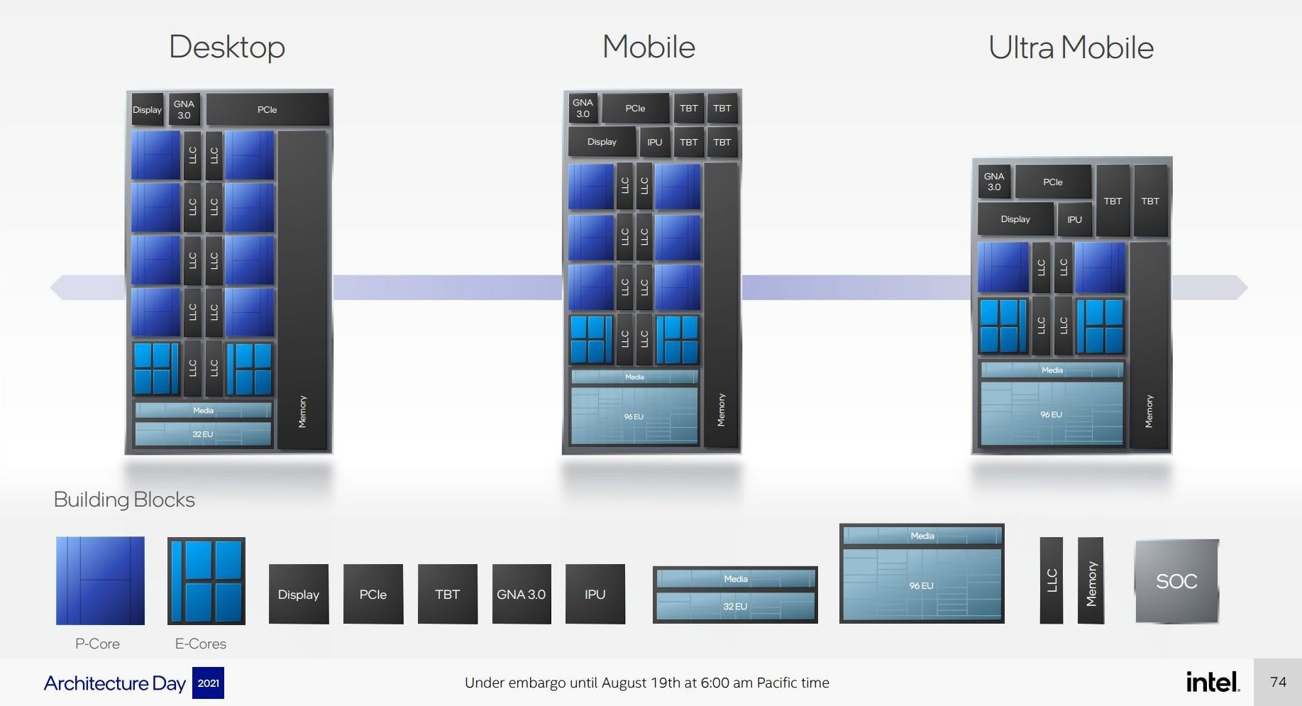
Here it shows that four E-cores takes up the same physical space as one P-core, but also that the desktop hardware will at most have 32 EUs (Execution Units) for Xe-LP graphics (same as the previous generation), while both of the mobile processors will offer 96 physical EUs that may be disabled down based on the specific line item in the product stack.
All three processors will feature Intel’s next generation Gaussian Neural Accelerator (GNA 3.0) for minor low power AI tasks, a display engine, and some level of PCIe, however the desktop processor will have more. Only the mobile processors will get an Image Processing Unit (IPU), and Thunderbolt 4 (TBT), and here the big UP3 mobile processor gets four ports of Thunderbolt whereas the smaller UP4 will only get two. The desktop processor will not have any native Thunderbolt connectivity.
A bit more info on the Desktop Processor IO and Interconnect
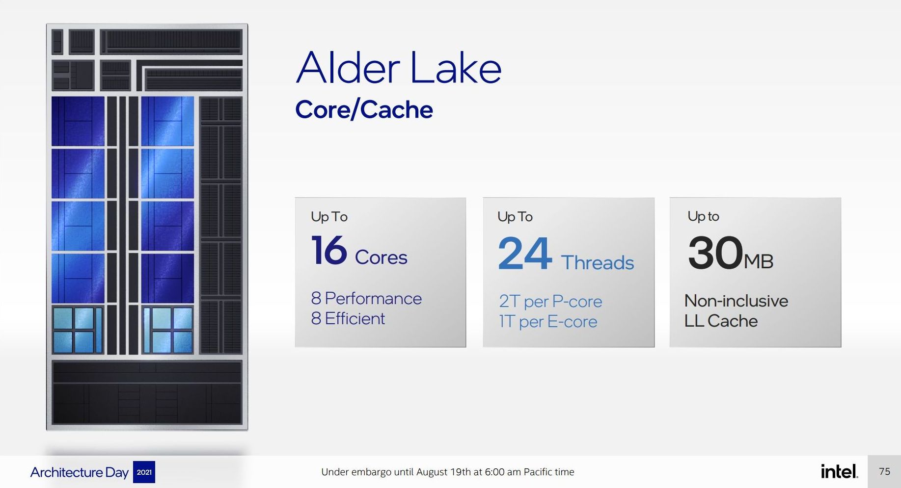
We’ll cover a bit more detail about the core designs later in this article, but Intel did showcase some of the information on the desktop processor. It confirmed explicitly that there would be 16 total cores and 24 threads, with up to 30 MB of non-inclusive last level/L3 cache.
In contrast to previous iterations of Intel’s processors, the desktop processor will support all modern standards: DDR5 at 4800 MT/s, DDR4-3200, LPDDR5-5200, and LPDDR4X-4266. Alongside this the processor will enable dynamic voltage-frequency scaling (aka turbo) and offer enhanced overclocking support. What exactly that last element means we’re unclear of at this point.
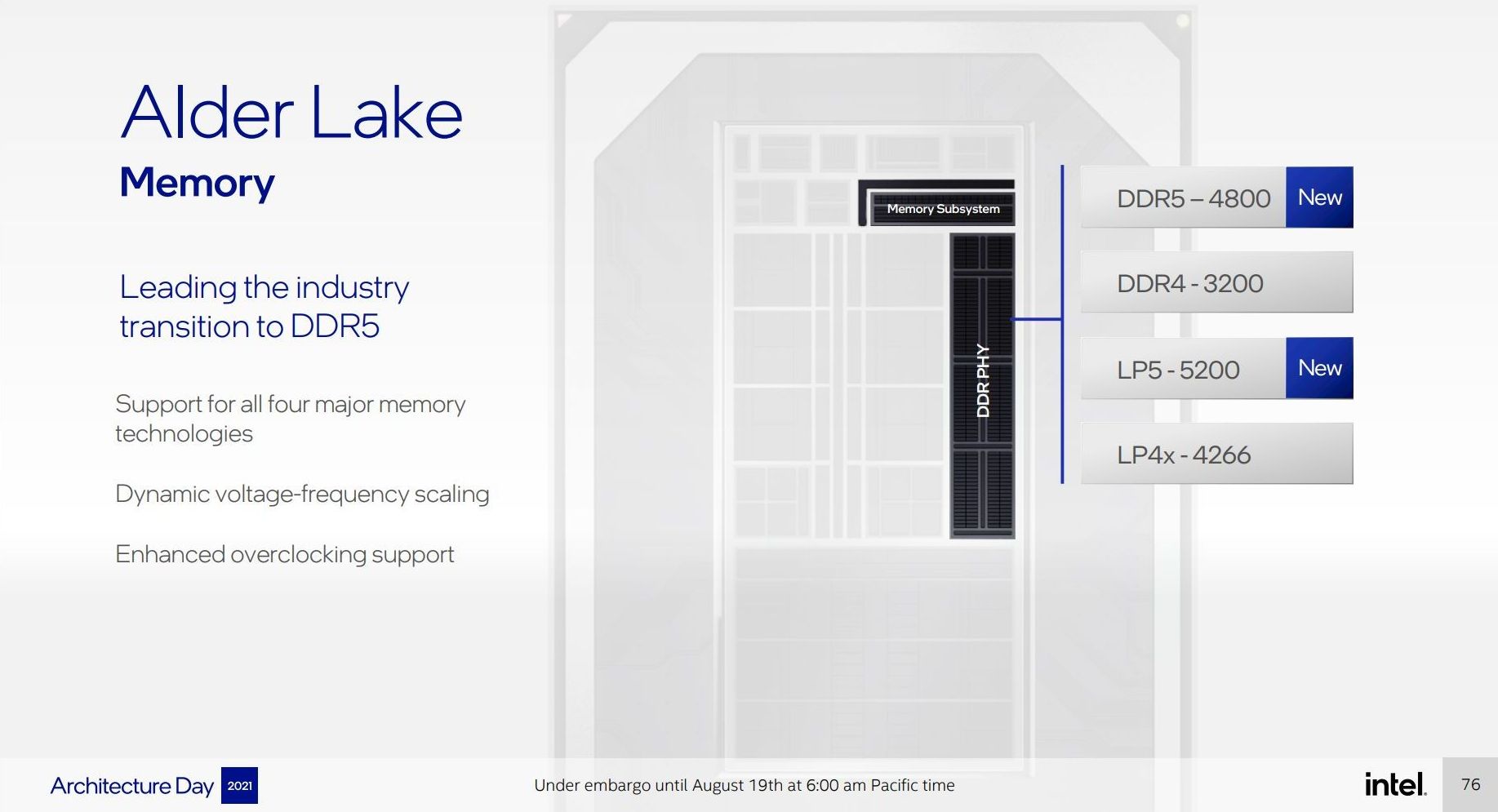
Intel confirmed that there will not be separate core designs with different memory support – all desktop processors will have a memory controller that can do all four standards. What this means is that we may see motherboards with built-in LPDDR5 or LPDDR4X rather than memory slots if a vendor wants to use LP memory, mostly likely in integrated small form factor designs but I wouldn’t put it past someone like ASRock to offer a mini-ITX board with built in LPDDR5. It was not disclosed what memory architectures the mobile processors will support, although we do expect almost identical support.
On the PCIe side of things, Alder Lake’s desktop processor will be supporting 20 lanes of PCIe, and this is split between PCIe 4.0 and PCIe 5.0.
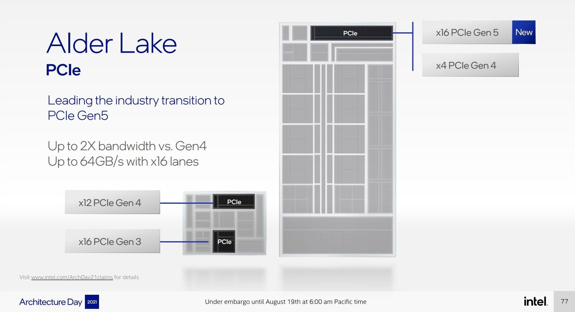
The desktop processor will have sixteen lanes of PCIe 5.0, which we expect to be split as x16 for graphics or as x8 for graphics and x4/x4 for storage. This will enable a full 64 GB/s bandwidth. Above and beyond this are another four PCIe 4.0 lanes for more storage. As PCIe 5.0 NVMe drives come to market, users may have to decide if they want the full PCIe 5.0 to the discrete graphics card or not
Intel also let it be known that the top chipset for Alder Lake on desktop now supports 12 lanes of PCIe 4.0 and 16 lanes of PCIe 3.0. This will allow for additional PCIe 4.0 devices to use the chipset, reducing the number of lanes needed for items like 10 gigabit Ethernet controllers or anything a bit spicier. If you ever thought your RGB controller could use more bandwidth, Intel is only happy to provide.
Intel did not disclose the bandwidth connectivity between the CPU and the chipset, though we believe this to be at least PCIe 4.0 x4 equivalent, if not higher.
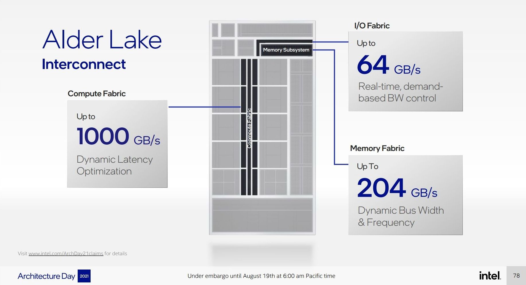
The Alder Lake processor retains the dual-bandwidth ring we saw implemented in Tiger Lake, enabling 1000 GB/s of bandwidth. We learned from asking Intel in our Q&A that this ring is fully enabled regardless of whether the P-cores or E-cores are being used – Intel can disable one of the two rings when less bandwidth is needed, which would save power, however based on previous testing this single ring could end up drawing substantial power compared to the E-cores in low power operation. (This may be true in the mobile processors as well, which would have knock on effects for mobile battery life.)
The 64 GB/s of IO fabric is in line with the PCIe 5.0 x16 numbers we saw above, however the 204 GB/s of memory fabric bandwidth is a confusing number. Alder Lake features a 128-bit memory bus, which allows for 4x 32-bit DDR5 channels (DDR5 has two 32-bit channels per module, so 2 modules still), however in order to reach 204 GB/s in that configuration requires DDR5-12750; Intel has rated the processor only at DDR5-4800, less than half that, so it is unclear where this 204 GB/s number comes from. For perspective, Intel’s Ice Lake does 204.8 GB/s, and that’s a high-power server platform with 8 channels of DDR4-3200.
This final slide mentions TB4 and Wi-Fi 6E, however as with previous desktop processors, these are derived from controllers attached to the chipset, and not in the silicon itself. The mobile processors will have TBT integrated, but the desktop processor does not.
This slide also mentions Intel Thread Director, which we want to address on the next page before we get to the microarchitecture analysis.


223 Comments
View All Comments
name99 - Saturday, August 21, 2021 - link
As always the devil is in the details :-)Basic loop buffers, as in the LSD (introduced one gen before Nehalem, with Core2) have been with us forever, including early ARM chips and the early PA Semi chips, going on to Apple Swift.
But the basic loop buffer can not deal with branches (because part of the system is to switch off branch prediction!). Part of what makes the Apple scheme interesting and exceptional is that it's this graduated scheme that manages to extract much of the energy win from the repetition of loops while being able to cover a much wider variety of loops including those with (not too awful) patterns of function calls and branches.
Comparing details is usually unhelpful because different architectures have different concerns; obviously x86 has decode+variable length concerns which is probably THE prime concern for how their structure their attempts to extract performance and energy savings from loops,
On the Apple side, I would guess that Mapping (specifically detecting dependencies within a Decode group of 8 instructions, ie what register written by instruction A is immediately read by successor instruction B) is a high-energy task, and a future direction for all these loop techniques on the Apple side might be to somehow save these inter-instruction-dependencies in the loop storage structure? This is, obviously, somewhat different from Intel or AMD's prime concern with their loops, given that even now they max out at only 5 (perhaps soon 6) wide in the mapping stage, and don't need to know as much for mapping because they don't do as much zero-cycle work in the stage right after Mapping.
GeoffreyA - Sunday, August 22, 2021 - link
Thanks. I suppose storing the dependancy information would be of use even in non-loop cases, because of the amount of work it takes. Then again, it might add greater complexity, which is always a drawback.mode_13h - Sunday, August 22, 2021 - link
> I would guess that Mapping (specifically detecting ... what register written by> instruction A is immediately read by successor instruction B) is a high-energy task
So, do you foresee some future ISA trying to map these out at compile-time, like Intel's ill-fated EPIC tried to do? On the one hand, it bloats the instruction size with redundant information. On the other, it would save some expensive lookups, at runtime. I guess you could boil it down to a question of whether it takes more energy for those bits to come in from DRAM and traverse the cache hierarchy vs. doing more work inside the core.
The other idea I have is that if the CPU stores some supplemental information in its i-cache, then why not actually flush that out to L3 & DRAM, rather than recompute it each time? The OS would obviously have to provide the CPU with a private data area, sort of like a shadow code segment, but at least the ISA wouldn't have to change.
mode_13h - Saturday, August 21, 2021 - link
Thanks. Very nice incremental explanation of a loop buffer, trace cache, and L0.> n-way set-associative cache means you now have, n slots associated with a given index.
> So if you have 8 slots, you can hold 8 lines with that same index,
> ie 8 addresses with those same middle bits.
> BUT how do you know WHICH of those 8 lines you want?
Yeah, I know how a set-associative cache works. The simplistic explanation is that there's a n-entry CAM (Content-Addressable Memory) which holds the upper bits of the addresses (I think what you're calling Tags) for each cache line in a set. So, a cache lookup involves up to n (I suppose 8, in this case) comparisons against those upper bits, to find out if any of them match the requested address. And, ideally, we want the hardware to do all those comparisons in parallel, so it can give a quicker answer where our data is (or fetch it, if the cache doesn't have it).
Even at that level, cache is something not enough software developers know about. It's really easy to thrash a normal set-associative cache. Just create a 2D array with a width that's a factor or an integral multiple of a cache set size and do a column-traversal. If you're lucky, your entire array fits in L3. If not... :(
> which of these 8 possible lines is of interest is called a WAY.
Where I first learned about CPU caches, they called it a set. So, an 8-way set-associative cache had 8 sets.
> by storing the cache way, you can access a cache with the speed ...
> and energy ... of a direct-mapped cache.
Yup. That's what I thought you were saying. So, the way/set + offset is basically an absolute pointer into the cache. And a bonus is that it only needs as many bits as the cache size, rather than a full address. So, a 64k cache would need only 16 bits to uniquely address any content it holds.
GeoffreyA - Thursday, August 19, 2021 - link
I believe the reservation station is that portion which contains the scheduler and physical register files. In Intel, it's been unified since P6, compared to AMD's split/distributed scheduler design and, I think, Netburst.name99 - Thursday, August 19, 2021 - link
"Intel is noting that they’re doing an increased amount of dependency resolution at the allocation stage, actually eliminating instructions that otherwise would have to actually emitted to the back-end execution resources."Again presumably this means "executing" instructions at Rename (or earlier) rather than as actual execution.
Apple examples are
- handling some aspects of branches (for unconditional branches) at Decode
- zero cycle move. This means you treat a move from one register to another by creating a second reference to the underlying physical register. Sounds obvious, the trick is tracking how many references now exist to a given physical register and when it can be freed. It's tricky enough that Apple have gone through three very different schemes so far.
- zero cycle immediates. The way Apple handle this is a separate pool of ~40 integer registers dedicated to handling MOV xn, # (ie load xn with immediate value #), and the instruction is again handled to Rename.
Intel could do the same.They already do this for zero idioms, of course.
- then there are weirder cases like value prediction where again you insert the value into the target register at Rename. The instruction still has to be validated (hence executed in some form) but the early insertion improves. Apple does this for certain patterns of loads, but the details are too complicated for here.
mode_13h - Friday, August 20, 2021 - link
Thanks again!name99 - Thursday, August 19, 2021 - link
"Someone please remind us what a reservation station is?"After an instruction is decoded it passes through Rename where resources it will need later (like a destination register, or a load/store queue entry) are allocated.
Then it is placed in a Scheduling Queue. It sits in the queue until its dependencies are resolved (ie ADD x0, x1, x2 cannot execute until the values of x1 and x2 are known.
This Scheduling Queue is also called a Reservation Station.
There is a huge dichotomy in design here. Intel insists on using a single such queue, everyone else uses multiple queues. Apple have a queue per execution unit, ala https://twitter.com/dougallj/status/13739734787312... (this is not 100% correct, but good enough).
The problem with a large queue is meeting cycle time. The problem with multiple queues is that they can get unbalanced. It's sad if you are executing integer only code and can't use the FP queue slots. Even worse is if you have one of your integer queues totally full, and the others empty, so only that one queue dispatches work per cycle.
Apple solve these in a bunch of ways.
First note the Dispatch Buffer in front of the Queues. This accepts instructions up to 8-wide per cycle from Rename, and sends as many as possible to the Scheduling Queues. It engages in load balancing to make sure that queues are always as close to evenly filled as possible.
Secondly the most recent Apple designs pair the Scheduling Queues so that, ideally, each queue issues one instruction, but if a Queue cannot find a runnable instruction, it will accept the second choice runnable candidate from its paired queue.
Queues and scheduling are actually immensely complicated. You have hundreds of instructions, all of which could depend in principle on any earlier instruction, so how do track (at minimal area and energy) all these dependencies? Apple appears to use a Matrix Scheduler with a TRULY ASTONISHINGLY CLEVER dependency scheme. A lot about the M1 impresses me, but if I had to choose one thing it might be this.
It's way too complicated to describe here, but among the things you need to bear in mind are
- you want to track which instructions depend on which
- you want to track the age of instructions (so that when multiple instructions are runnable, earliest go first)
- you need to handle Replay. I won't describe this here, but for people who know what it is, Apple provide
+ cycle-accurate Replay (no randomly retrying every four cycles till you finally succeed!) AND, most amazingly
+ perfect DEMAND Replay (only the instructions, down a chain of dependencies) that depended on a Replay are in turn Replayed (and, again, at the cycle accurate time)
+ if you think that's not amazing enough, think about what this implies for value prediction, and how much more aggressive you can be if the cost of a mispredict is merely a cycle-accurate on-demand Replay rather than a Flush!!!
mode_13h - Friday, August 20, 2021 - link
Wow, you're on a roll!name99 - Thursday, August 19, 2021 - link
"> full-line-write predictive bandwidth optimisation ... where the core can greatly improve> bandwidth by avoiding RFO reads of cache lines that are going to be fully rewritten"
Of course this is one of those "about time" optimizations :-)
Apple (it's SO MUCH EASIER with a decent memory model, so I am sure also ARM) have had this for years of course. But improvements to it include
- treat all-zero lines as special cases that are tagged in L2/SLC but don't require transferring data on the NoC. Intel had something like this in IceLake that, after some time, they switched off with microcode update.
- store aggregation is obvious and easy if your memory model allows it. But Apple also engages in load aggregation (up to a cache line width) for uncachable data. I'm not sure what the use cases of this are (what's still uncachable in a modern design? reads rather than DMA from PCIe?) but apparently uncachable loads and stores remain a live issue; Apple is still generating patents about them even now.
- Apple caches all have a bit per line that indicates whether this line should be treated as streaming vs LRU. Obviously any design that provides non-temporal loads/stores needs something like that, but the Apple scheme also allows you to mark pages (or range registers, which are basically BATs -- yes PPC BATs are back, baby!) as LRU or streaming, then the system will just do the right thing whether that data is accessed by load/stores, prefetch or whatever else.
BTW, just as an aside, Apple's prefetchers start at the load-store unit, not the L1. Meaning they see the VIRTUAL address stream.) This in turn means they can cross page boundaries (and prefetch TLB entries for those boundary crossings). They're also co-ordinated so that each L1 is puppeting what it want the L2 prefetcher to do for it, rather than having L1 and L2 prefetchers working independently and hoping that it kinda sorta results in what you want. And yes, of course, tracking prefetching efficiency and throttling when appropriate have always been there.