Apple Announces M1 Pro & M1 Max: Giant New Arm SoCs with All-Out Performance
by Andrei Frumusanu on October 18, 2021 4:00 PM EST- Posted in
- Mobile
- Apple
- Laptops
- Apple M1
- Apple M1 Pro
- Apple M1 Max
Today’s Apple Mac keynote has been very eventful, with the company announcing a new line-up of MacBook Pro devices, powered by two different new SoCs in Apple’s Silicon line-up: the new M1 Pro and the M1 Max.
The M1 Pro and Max both follow-up on last year’s M1, Apple’s first generation Mac silicon that ushered in the beginning of Apple’s journey to replace x86 based chips with their own in-house designs. The M1 had been widely successful for Apple, showcasing fantastic performance at never-before-seen power efficiency in the laptop market. Although the M1 was fast, it was still a somewhat smaller SoC – still powering devices such as the iPad Pro line-up, and a corresponding lower TDP, naturally still losing out to larger more power-hungry chips from the competition.
Today’s two new chips look to change that situation, with Apple going all-out for performance, with more CPU cores, more GPU cores, much more silicon investment, and Apple now also increasing their power budget far past anything they’ve ever done in the smartphone or tablet space.
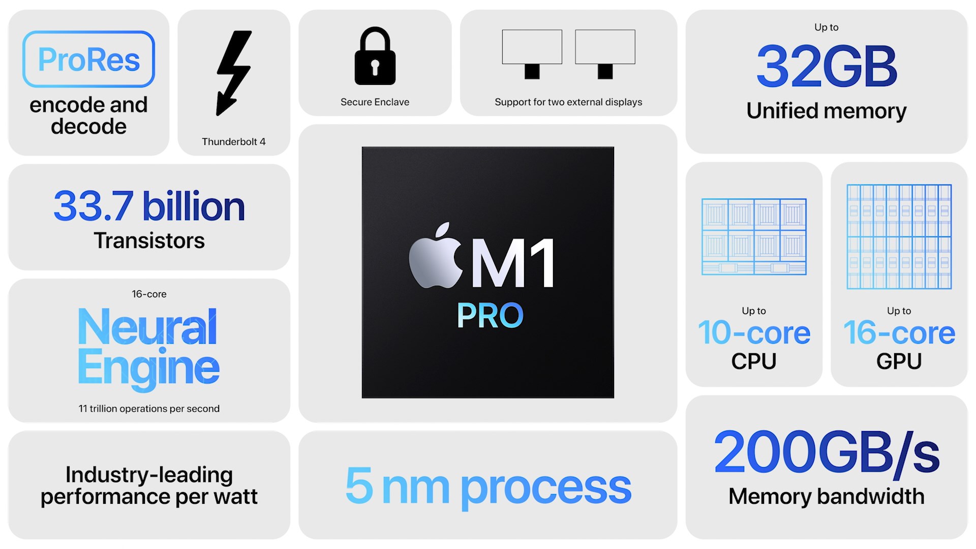
The M1 Pro: 10-core CPU, 16-core GPU, 33.7bn Transistors in 245mm²
The first of the two chips which were announced was the so-called M1 Pro – laying the ground-work for what Apple calls no-compromise laptop SoCs.
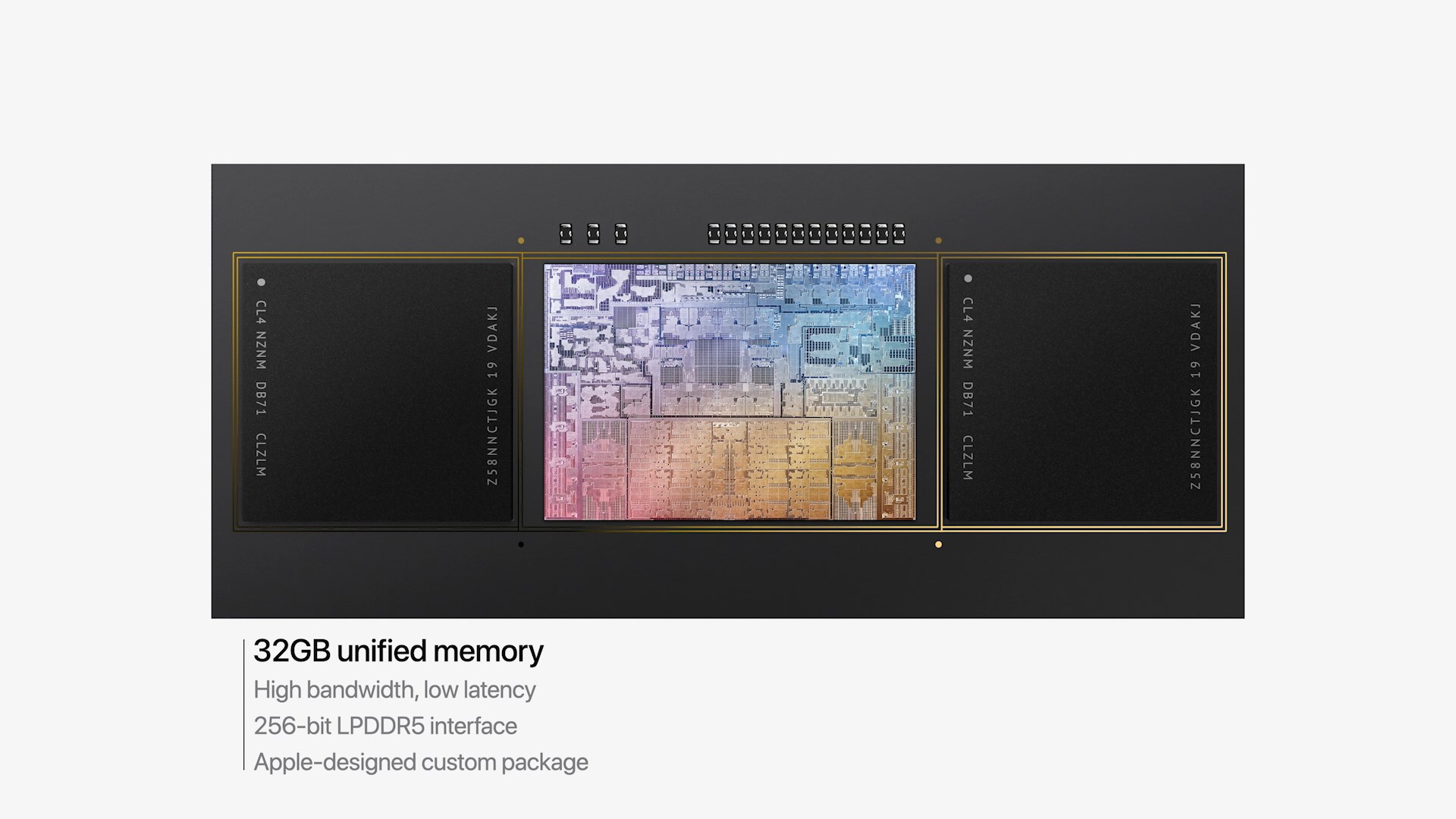
Apple started off the presentation with a showcase of the packaging, there the M1 Pro is shown to continue to feature very custom packaging, including the still unique characteristic that Apple is packaging the SoC die along with the memory dies on a single organic PCB, which comes in contrast to other traditional chips such as from AMD or Intel which feature the DRAM dies either in DIMM slots, or soldered onto the motherboard. Apple’s approach here likely improves power efficiency by a notable amount.
The company divulges that they’ve doubled up on the memory bus for the M1 Pro compared to the M1, moving from a 128-bit LPDDR4X interface to a new much wider and faster 256-bit LPDDR5 interface, promising system bandwidth of up to 200GB/s. We don’t know if that figure is exact or rounded, but an LPDDR5-6400 interface of that width would achieve 204.8GB/s.
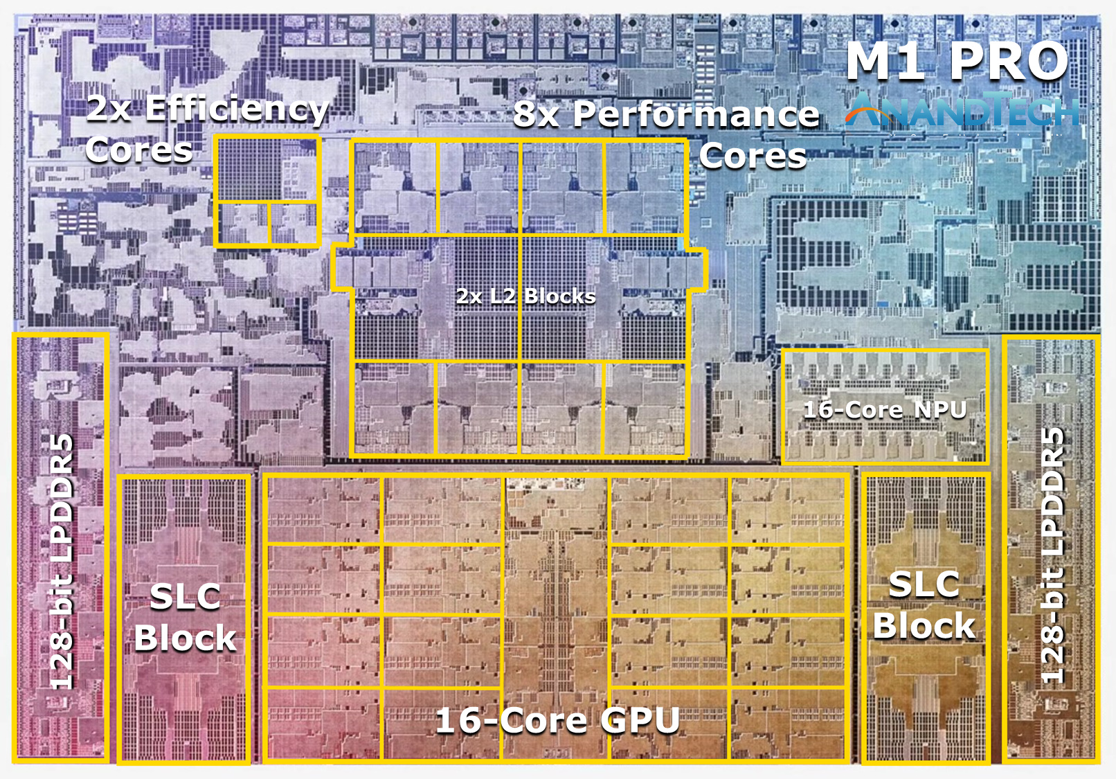
In a much-appreciated presentation move, Apple actually showcased the die shots of both the M1 Pro and M1 Max, so we can have an immediate look at the chip’s block layout, and how things are partitioned. Let’s start off with the memory interfaces, which are now more consolidated onto two corners of the SoC, rather than spread out along two edges like on the M1. Because of the increased interface width, we’re seeing quite a larger portion of the SoC being taken up by the memory controllers. However, what’s even more interesting, is the fact that Apple now apparently employs two system level cache (SLC) blocks directly behind the memory controllers.
Apple’s system level cache blocks have been notable as they serve the whole SoC, able to amplify bandwidth, reduce latency, or simply just save power by avoiding memory transactions going off-chip, greatly improving power efficiency. This new generation SLC block looks quite a bit different to what we’ve seen on the M1. The SRAM cell areas look to be larger than that of the M1, so while we can’t exactly confirm this right now, it could signify that each SLC block has 16MB of cache in it – for the M1 Pro that would mean 32MB of total SLC cache.
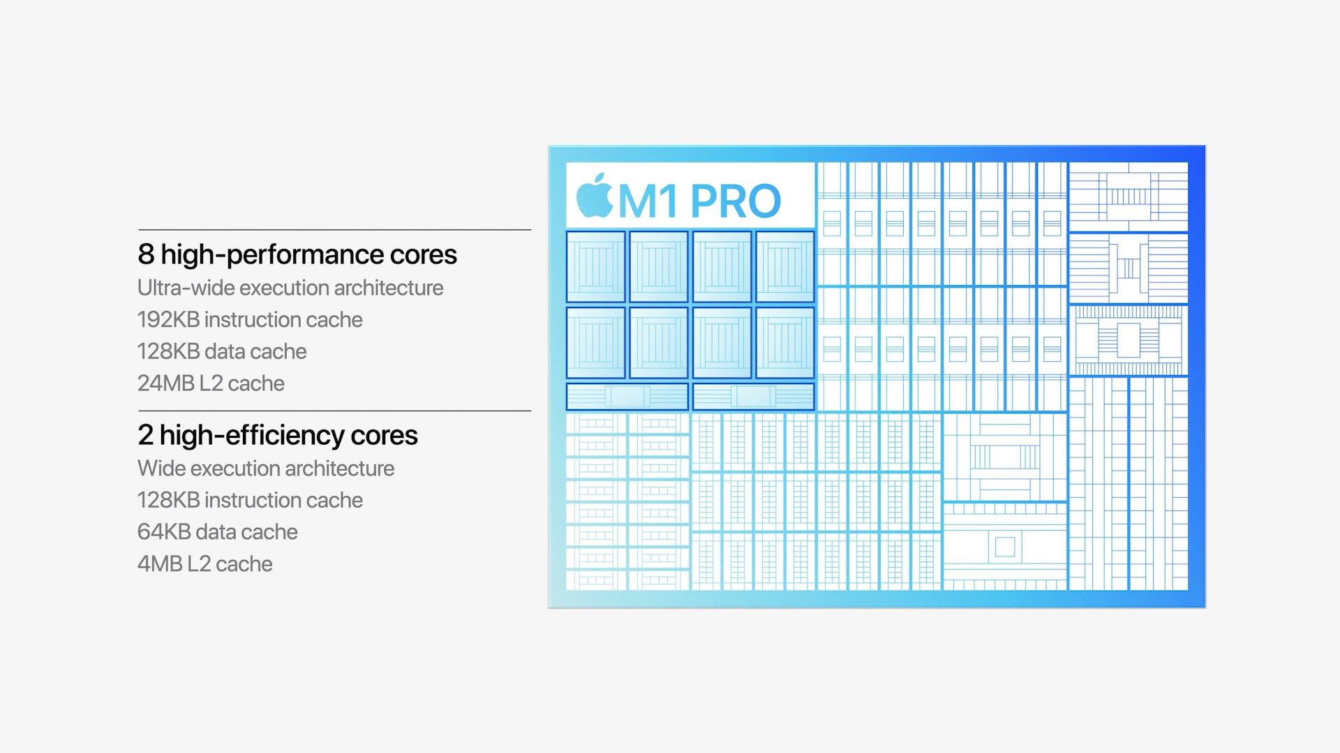
On the CPU side of things, Apple has shrunk the number of efficiency cores from 4 to 2. We don’t know if these cores would be similar to that of the M1 generation efficiency cores, or if Apple adopted the newer generation IP from the A15 SoC – we had noted that the new iPhone SoC had some larger microarchitectural changes in that regard.
On the performance core side, Apple has doubled things up to 8 cores now. Apple’s performance cores were extremely impressive on the M1, however were lagging behind other 8-core SoCs in terms of multi-threaded performance. This doubling up of the cores should showcase immense MT performance boosts.
On the die shot, we’re seeing that Apple is seemingly mirroring two 4-core blocks, with the L2 caches also being mirrored. Although Apple quotes 24MB of L2 here, I think it’s rather a 2x12MB setup, with an AMD core-complex-like setup being used. This would mean that the coherency of the two performance clusters is going over the fabric and SLC instead. Naturally, this is speculation for now, but it’s what makes most sense given the presented layout.
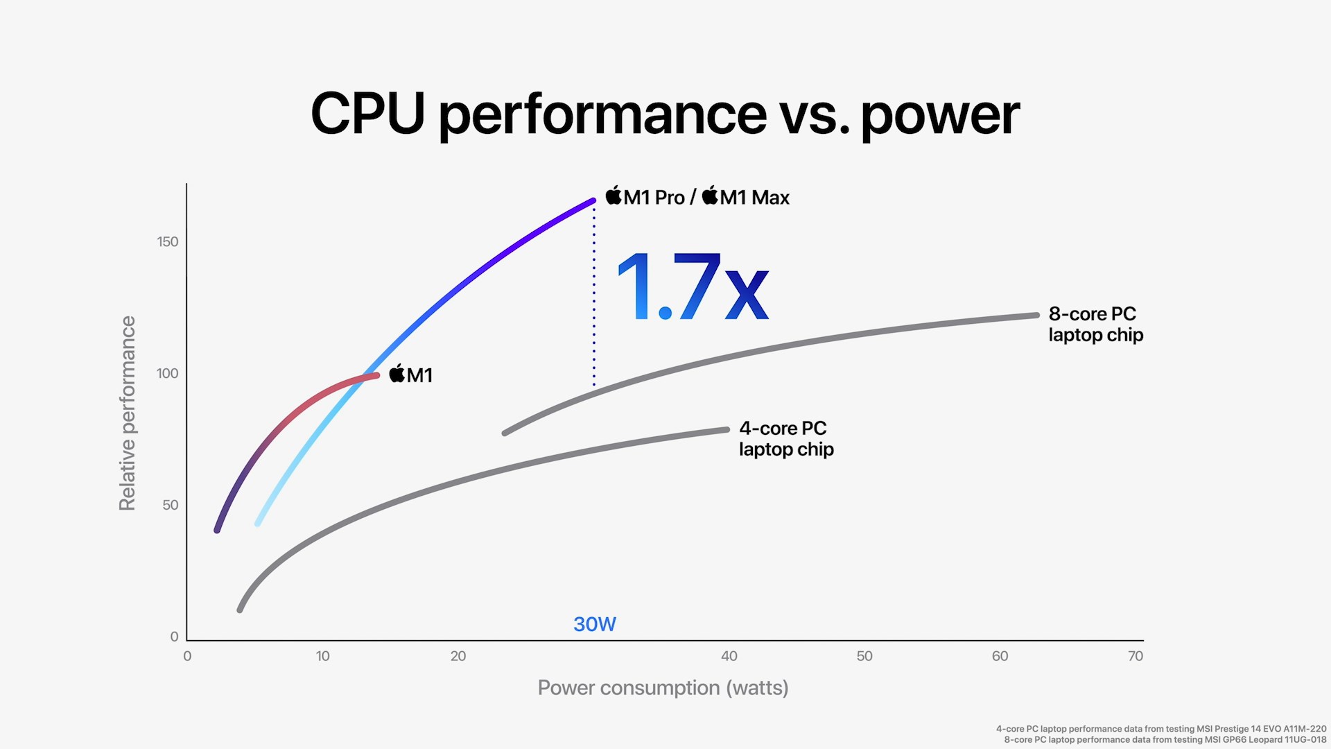
In terms of CPU performance metrics, Apple made some comparisons to the competition – in particular the SKUs being compared here were Intel’s Core i7-1185G7, and the Core i7-11800H, 4-core and 8-core variants of Intel’s latest Tiger Lake 10nm 'SuperFin' CPUs.
Apple here claims, that in multi-threaded performance, the new chips both vastly outperform anything Intel has to offer, at vastly lower power consumption. The presented performance/power curves showcase that at equal power usage of 30W, the new M1 Pro and Max are 1.7x faster in CPU throughput than the 11800H, whose power curve is extremely steep. Whereas at an equal performance levels – in this case using the 11800H's peak performance – Apple says that the new M1 Pro/Max achieves the same performance with 70% lower power consumption. Both figures are just massive discrepancies and leap ahead of what Intel is currently achieving.
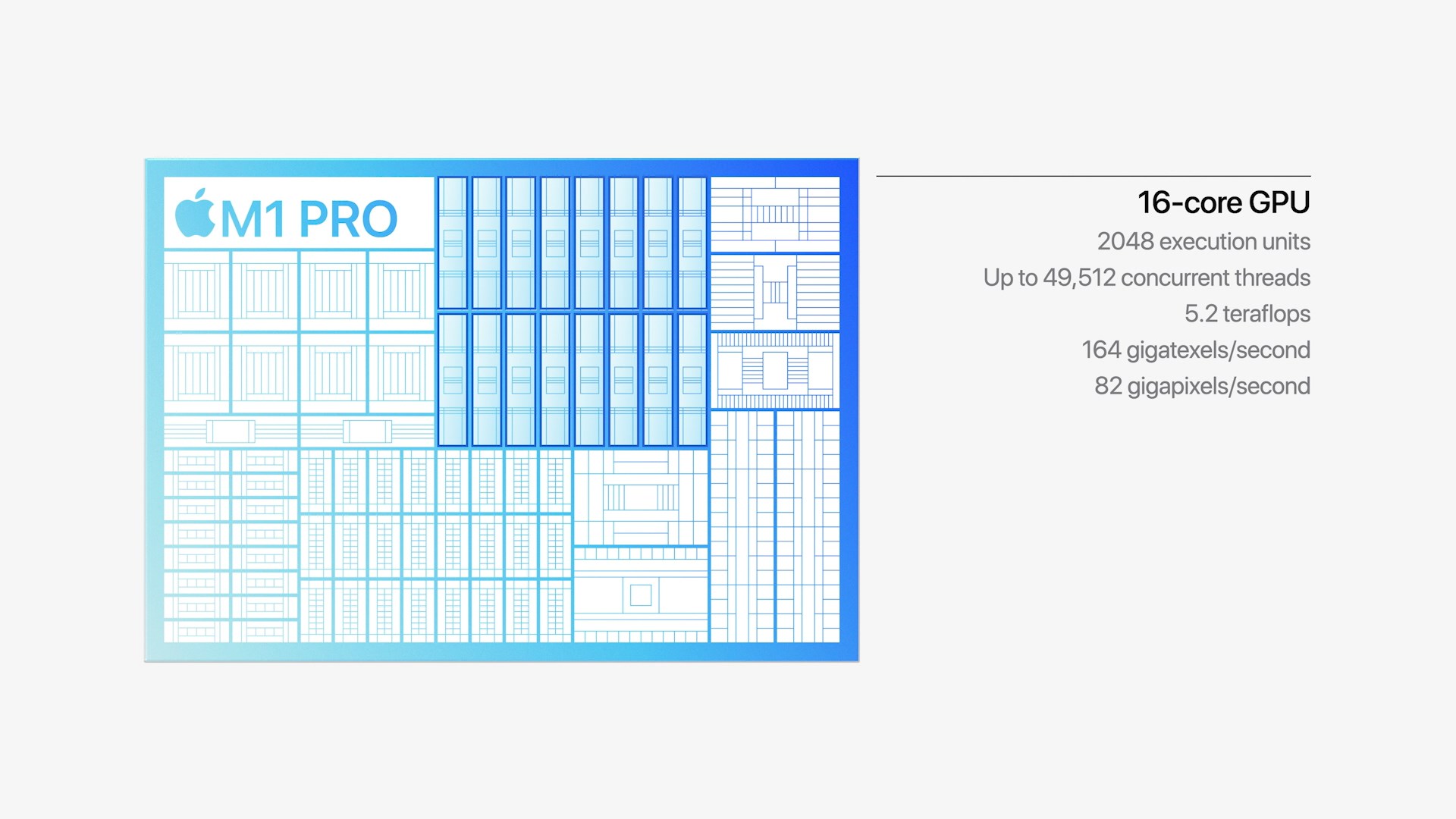
Alongside the powerful CPU complexes, Apple is also supersizing their custom GPU architecture. The M1 Pro now features a 16-core GPU, with an advertised compute throughput performance of 5.2 TFLOPs. What’s interesting here, is that this new much larger GPU would be supported by the much wider memory bus, as well as the presumably 32MB of SLC – this latter essentially acting similarly to what AMD is now achieving with their GPU Infinity Cache.
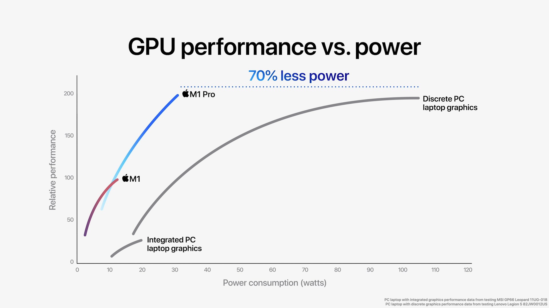
Apple’s GPU performance is claimed to vastly outclass any previous generation competitor integrated graphics performance, so the company opted to make direct comparisons to medium-end discrete laptop graphics. In this case, pitting the M1 Pro against a GeForce RTX 3050 Ti 4GB, with the Apple chip achieving similar performance at 70% less power. The power levels here are showcased as being at around 30W – it’s not clear if this is total SoC or system power or Apple just comparing the GPU block itself.

Alongside the GPU and CPUs, Apple also noted their much-improved media engine, which can now handle hardware accelerated decoding and encoding of ProRes and ProRes RAW, something that’s going to be extremely interesting to content creators and professional videographers. Apple Macs have generally held a good reputation for video editing, but hardware accelerated engines for RAW formats would be a killer feature that would be an immediate selling point for this audience, and something I’m sure we’ll hear many people talk about.
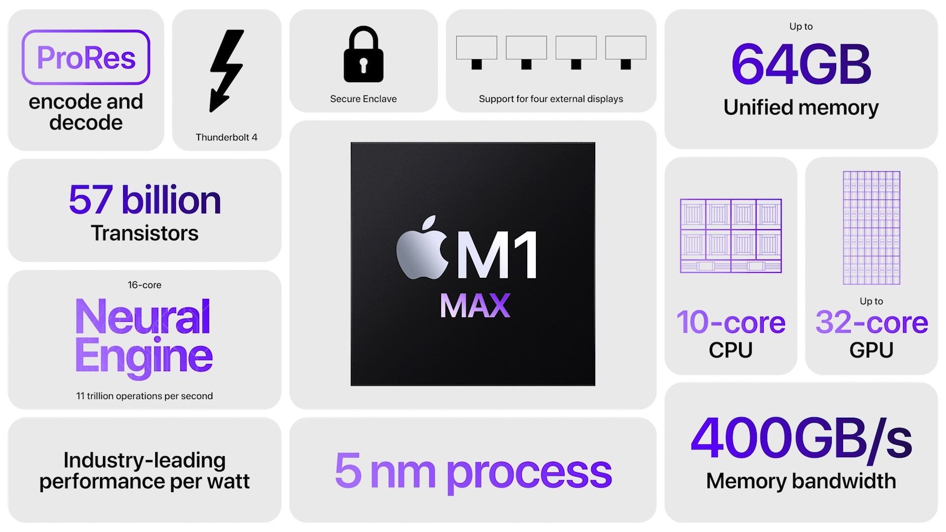
The M1 Max: A 32-Core GPU Monstrosity at 57bn Transistors & 432mm²
Alongside the M1 Pro, Apple also announced a bigger brother – the M1 Max. While the M1 Pro catches up and outpaces the laptop competition in terms of performance, the M1 Max is aiming at delivering something never-before seen: supercharging the GPU to a total of 32 cores. Essentially it’s no longer an SoC with an integrated GPU, rather it’s a GPU with an SoC around it.
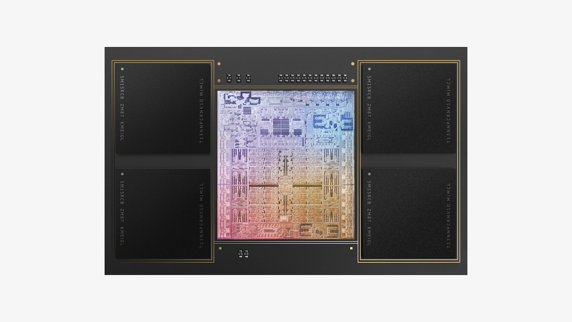
The packaging for the M1 Max changes slightly in that it’s bigger – the most obvious change is the increase of DRAM chips from 2 to 4, which also corresponds to the increase in memory interface width from 256-bit to 512-bit. Apple is advertising a massive 400GB/s of bandwidth, which if it’s LPDDR5-6400, would possibly be more exact at 409.6GB/s. This kind of bandwidth is unheard of in an SoC, but quite the norm in very high-end GPUs.
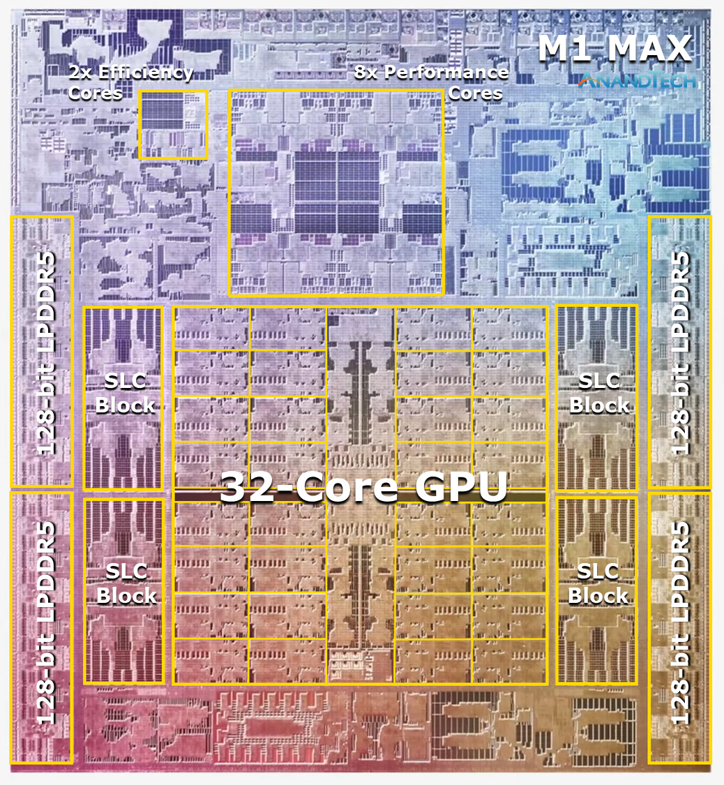
On the die shot of the M1 Max, things look quite peculiar – first of all, the whole top part of the chip above the GPU essentially looks identical to the M1 Pro, pointing out that Apple is reusing most of the design, and that the Max variant simply grows downwards in the block layout.
The additional two 128-bit LPDDR5 blocks are evident, and again it’s interesting to see here that they’re also increasing the number of SLC blocks along with them. If indeed at 16MB per block, this would represent 64MB of on-chip generic cache for the whole SoC to make use of. Beyond the obvious GPU uses, I do wonder what the CPUs are able to achieve with such gigantic memory bandwidth resources.
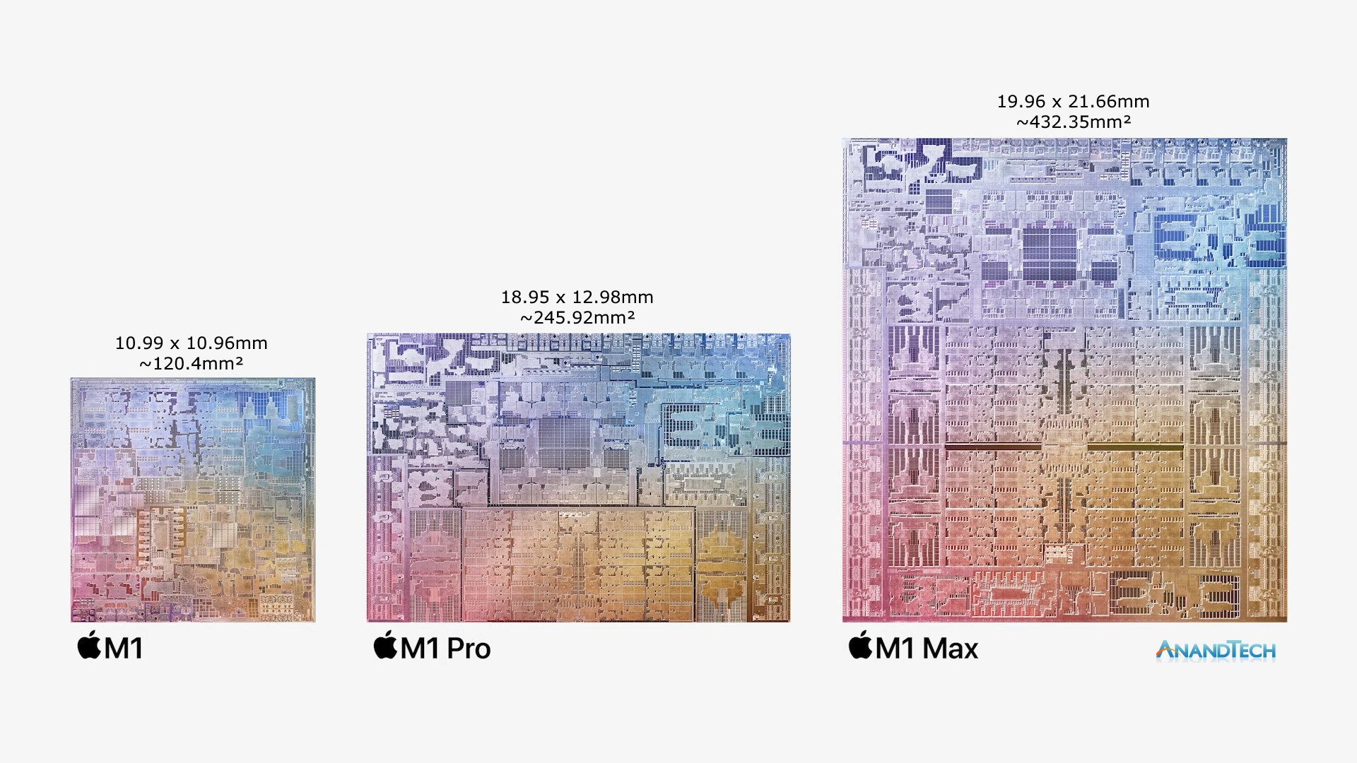
The M1 Max is truly immense – Apple disclosed the M1 Pro transistor count to be at 33.7 billion, while the M1 Max bloats that up to 57 billion transistors. AMD advertises 26.8bn transistors for the Navi 21 GPU design at 520mm² on TSMC's 7nm process; Apple here has over double the transistors at a lower die size thanks to their use of TSMC's leading-edge 5nm process. Even compared to NVIDIA's biggest 7nm chip, the 54 billion transistor server-focused GA100, the M1 Max still has the greater transistor count.
In terms of die sizes, Apple presented a slide of the M1, M1 Pro and M1 Max alongside each other, and they do seem to be 1:1 in scale. In which case, the M1 we already know to be 120mm², which would make the M1 Pro 245mm², and the M1 Max about 432mm².

Most of the die size is taken up by the 32-core GPU, which Apple advertises as reaching 10.4TFLOPs. Going back at the die shot, it looks like Apple here has basically mirrored their 16-core GPU layout. The first thing that came to mind here was the idea that these would be 2 GPUs working in unison, but there does appear to be some shared logic between the two halves of the GPU. We might get more clarity on this once we see software behavior of the system.
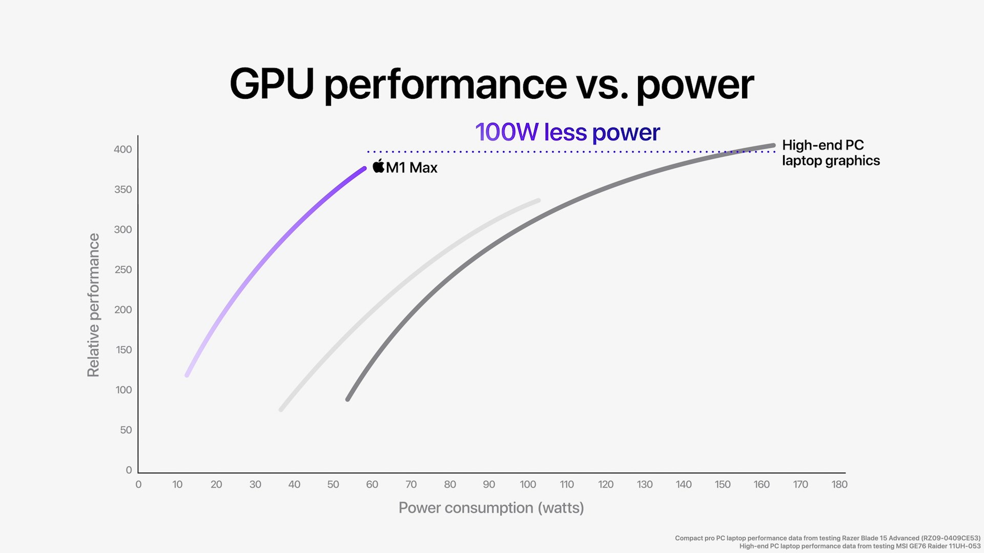
In terms of performance, Apple is battling it out with the very best available in the market, comparing the performance of the M1 Max to that of a mobile GeForce RTX 3080, at 100W less power (60W vs 160W). Apple also includes a 100W TDP variant of the RTX 3080 for comparison, here, outperforming the NVIDIA discrete GPU, while still using 40% less power.
Today's reveal of the new generation Apple Silicon has been something we’ve been expecting for over a year now, and I think Apple has managed to not only meet those expectations, but also vastly surpass them. Both the M1 Pro and M1 Max look like incredibly differentiated designs, much different than anything we’ve ever seen in the laptop space. If the M1 was any indication of Apple’s success in their silicon endeavors, then the two new chips should also have no issues in laying incredible foundations for Apple’s Mac products, going far beyond what we’ve seen from any competitor.


373 Comments
View All Comments
Tomatotech - Thursday, October 21, 2021 - link
Apple press embargo lifts at 9am ET on Monday. Detailed reviews will hit a few seconds later.As far as SSD goes, it's either PCIe 3.0 x8 or PCIe 4.0 x 4 (I favour the latter).
I speculate there will be a Mac Pro with 4x these NVMe SSDs for a total of 30GB/s aggregate bandwidth to backing storage, either 32TB in total or 64TB total by the time it's released.
Tomatotech - Thursday, October 21, 2021 - link
* 32TB or 64TB, all soldered on a single motherboard with up to 4 Pro Max CPU packages also soldered on it. If slots are provided, which could just be slots on a daughtercard connected via TB4 to the main motherboard, then you could put additional NVMe drives on a riser or attach SATA drives for more storage. Hopefully the case will still provide somewhere to put them & keep the whole thing tidy.Ppietra - Thursday, October 21, 2021 - link
I would expect Apple to make a chiplet instead of soldering 4 different M1 Max packages onto the motherboard.ruthan - Thursday, October 21, 2021 - link
Its shame that Apple is only company whose tried to make beefier ARM chip.. It would be interesting, how would be virtualization performace with Windows machine, if it would be faster than real x86 Windows machine, it would clear victory otherwise it would be only great for MacOS ecosystem behind their iron curtain..06GTOSC - Thursday, October 21, 2021 - link
Wondering what the yields are on the M1 Max.yitwail - Thursday, October 21, 2021 - link
I apologize if this was mentioned already but the diagrams don’t match the die photos, so the diagrams are just abstractions? Also, are all those performance vs power graphs idealized? Because all the curves are so smooth.mvalborg - Friday, October 22, 2021 - link
Anand review of Apple are abysmally bad. The former head Anand, of course being an Apple employee.. The people at Anand covering Apple are really nothing more than cheap Apple shills :-(Farfolomew - Saturday, October 23, 2021 - link
Ian Cuttress has mentioned that Anand La Shimpi has little to no interaction (let alone involvement) with Anandtech anymore. Apple doesn't need to pay sites for coverage when their products are just that good and every website comes to the same consensus. Time to step your game up, PCweb2dot0 - Saturday, October 23, 2021 - link
If you want to call someone a shill, please provide which part of Ian Cutress article on M1/M1Pro/Max is inaccurate.Which part of below stats are lies?
1) 400GB/s 32ch LDDR5-6400
2) 7.4GB/s SSD
3) 30W CPU TDP, 60W GPU TDP
How is the review bad? Or is it because your feelings are hurt that your AMD/Nvidia/Intel is not getting the Performance/Watt that Apple is producing?
Curious.
corinthos - Monday, October 25, 2021 - link
Just wait for Intel Awesome Lake release. It will TORCH M1 in 2026.