Apple's M1 Pro, M1 Max SoCs Investigated: New Performance and Efficiency Heights
by Andrei Frumusanu on October 25, 2021 9:00 AM EST- Posted in
- Laptops
- Apple
- MacBook
- Apple M1 Pro
- Apple M1 Max
Last week, Apple had unveiled their new generation MacBook Pro laptop series, a new range of flagship devices that bring with them significant updates to the company’s professional and power-user oriented user-base. The new devices particularly differentiate themselves in that they’re now powered by two new additional entries in Apple’s own silicon line-up, the M1 Pro and the M1 Max. We’ve covered the initial reveal in last week’s overview article of the two new chips, and today we’re getting the first glimpses of the performance we’re expected to see off the new silicon.
The M1 Pro: 10-core CPU, 16-core GPU, 33.7bn Transistors
Starting off with the M1 Pro, the smaller sibling of the two, the design appears to be a new implementation of the first generation M1 chip, but this time designed from the ground up to scale up larger and to more performance. The M1 Pro in our view is the more interesting of the two designs, as it offers mostly everything that power users will deem generationally important in terms of upgrades.
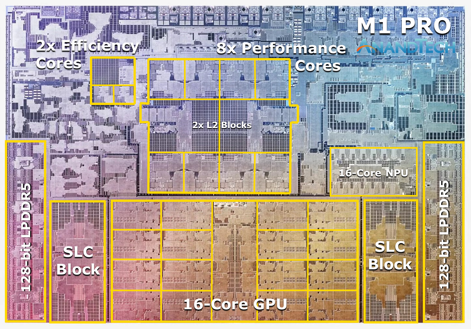
At the heart of the SoC we find a new 10-core CPU setup, in a 8+2 configuration, with there being 8 performance Firestorm cores and 2 efficiency Icestorm cores. We had indicated in our initial coverage that it appears that Apple’s new M1 Pro and Max chips is using a similar, if not the same generation CPU IP as on the M1, rather than updating things to the newer generation cores that are being used in the A15. We seemingly can confirm this, as we’re seeing no apparent changes in the cores compared to what we’ve discovered on the M1 chips.
The CPU cores clock up to 3228MHz peak, however vary in frequency depending on how many cores are active within a cluster, clocking down to 3132 at 2, and 3036 MHz at 3 and 4 cores active. I say “per cluster”, because the 8 performance cores in the M1 Pro and M1 Max are indeed consisting of two 4-core clusters, both with their own 12MB L2 caches, and each being able to clock their CPUs independently from each other, so it’s actually possible to have four active cores in one cluster at 3036MHz and one active core in the other cluster running at 3.23GHz.
The two E-cores in the system clock at up to 2064MHz, and as opposed to the M1, there’s only two of them this time around, however, Apple still gives them their full 4MB of L2 cache, same as on the M1 and A-derivative chips.
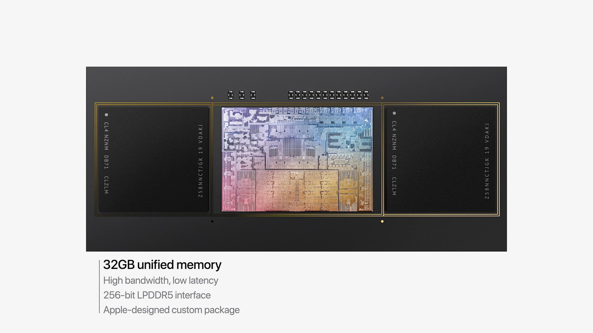
One large feature of both chips is their much-increased memory bandwidth and interfaces – the M1 Pro features 256-bit LPDDR5 memory at 6400MT/s speeds, corresponding to 204GB/s bandwidth. This is significantly higher than the M1 at 68GB/s, and also generally higher than competitor laptop platforms which still rely on 128-bit interfaces.
We’ve been able to identify the “SLC”, or system level cache as we call it, to be falling in at 24MB for the M1 Pro, and 48MB on the M1 Max, a bit smaller than what we initially speculated, but makes sense given the SRAM die area – representing a 50% increase over the per-block SLC on the M1.
The M1 Max: A 32-Core GPU Monstrosity at 57bn Transistors
Above the M1 Pro we have Apple’s second new M1 chip, the M1 Max. The M1 Max is essentially identical to the M1 Pro in terms of architecture and in many of its functional blocks – but what sets the Max apart is that Apple has equipped it with much larger GPU and media encode/decode complexes. Overall, Apple has doubled the number of GPU cores and media blocks, giving the M1 Max virtually twice the GPU and media performance.
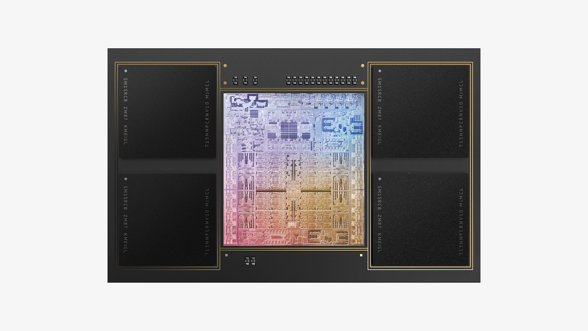
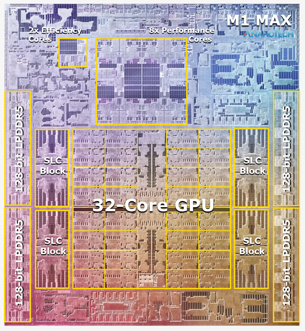
The GPU and memory interfaces of the chip are by far the most differentiated aspects of the chip, instead of a 16-core GPU, Apple doubles things up to a 32-core unit. On the M1 Max which we tested for today, the GPU is running at up to 1296MHz - quite fast for what we consider mobile IP, but still significantly slower than what we’ve seen from the conventional PC and console space where GPUs now can run up to around 2.5GHz.
Apple also doubles up on the memory interfaces, using a whopping 512-bit wide LPDDR5 memory subsystem – unheard of in an SoC and even rare amongst historical discrete GPU designs. This gives the chip a massive 408GB/s of bandwidth – how this bandwidth is accessible to the various IP blocks on the chip is one of the things we’ll be investigating today.
The memory controller caches are at 48MB in this chip, allowing for theoretically amplified memory bandwidth for various SoC blocks as well as reducing off-chip DRAM traffic, thus also reducing power and energy usage of the chip.
Apple’s die shot of the M1 Max was a bit weird initially in that we weren’t sure if it actually represents physical reality – especially on the bottom part of the chip we had noted that there appears to be a doubled up NPU – something Apple doesn’t officially disclose. A doubled up media engine makes sense as that’s part of the features of the chip, however until we can get a third-party die shot to confirm that this is indeed how the chip looks like, we’ll refrain from speculating further in this regard.


493 Comments
View All Comments
celeste_P - Tuesday, October 26, 2021 - link
Does any one know where can I find the policy about translating/reprinting the article? Do AnandTech allow such behavior? What are the policies that one needs to follow?This article is quite interesting and I want to translate/publish it on Chinese website to share with a broader range of people
colinstalter - Wednesday, October 27, 2021 - link
Why not just share the URL on the Chinese page? Do people in China not have translator functions built into their web browsers like Chrome does?celeste_P - Wednesday, October 27, 2021 - link
Of course they do XDBut as you can imagine, the quality of machine translation won't be that great, especially considering all these domain specific terms within this article.
ABR - Tuesday, October 26, 2021 - link
An excellent review.ajmas - Tuesday, October 26, 2021 - link
Given the number of games already available and running on iOS, I wonder how much work would be involved in making them available on macOS?As for effective performance, I am eagerly waiting to see what the real world tests reveal, since specs only say so much.
mandirabl - Wednesday, October 27, 2021 - link
As a developer, technically you don't have to do much, just re-compile the game and check another box (for Mac), basically.The problem is: iOS games are mostly touch-focused, whereas macOS is mouse-first. So they have to check if that translates without changing anything. If it does, it's a matter of a couple of minutes. If it doesn't translate well ... they have a choice to release it anyway or blocking access on macOS. Yes, developers have to actually decide against releasing their app/game for macOS - if they don't do anything in that regard, the app/game simply shows up in an App Store search on a Mac.
Kevin45 - Tuesday, October 26, 2021 - link
Apple's goal is very simple: If you are going to provide SW tools for Pro users of the MacOS platform, you write to Metal - period.It IS the most superior way to take advantage of what Apple has laid out to developers and Apple's Pro users absolutely want the HW tools they buy to be max'd out by the developers.
Apple has taken an approach Intel and AMD cannot. Unified memory design aside, Apple has looked at it's creative markets and developed sub-cores, which for this Creative focus segment, Apple markets as it's "Media Engine" which has hardware h.264 and hardware ProRes compute, which just crush these formats and codecs.
The argument "Yah, but the CPU and GPU cores aren't the most powerful that one can buy." is still. They don't need to be because they have dedicated cores to where the power needs to be. Sure, in a Wintel world, or Linux space, more powerful GPU and CPU cores is all they've got. So when talking those worlds indeed that's the correct argument. Not when talking Apple HW with Apple silicon.
Intel has fought nVIDIA to have their beefier and beefier cores do heavy lifting, while nVIDA wants the GPU to be the most important play in the mix. Apple has broken out their SoC into many sub-sets to meet the high compute needs of it's user base.
Now more than ever, developers that have drug their feet, need to get onboard. As companies continue to show off - such as Apple with FCP, Motion and Compressor optimized apps for the hardware, even DaVinci (niche player but powerful), they put pressure on other players such as sloth-boy Adobe, to get going and truly write for Apple's tools that take advantage of such well thought out HW + SW combo.
richardnpaul - Tuesday, October 26, 2021 - link
The article comes across a bit fanbioy. (yes, yes I know that this is usually the case here but I just wanted to say it out loud again). See below for why.You have covered in depth things like how the increased L3 design between Zen2 and 3 can cause big jumps in performance and what was missing here was discussion of how the 24/48MB cache between the memory interface impacts performance especially when using the GPU (we've seen this last year AMD's designs doing exactly this to improve performance of their designs by reducing the impact of calling out to the slow GDDR6 RAM.)
The GPU is nothing special. 10Tflops at 1.3GHz puts it around the same class as a Vega64, a 14nm design, which similarly used RAM packaged on an interposer with the GPU (being 14nm it was big, 5nm makes it much more reasonable). With the buffer cache I'd expect it might perform better, also the CPUs will bump up performance (just look at how much more FPS you get with Zen3 over Zen2 and with Zen3 with vcache it'll be another 15% more on top from exactly the same GPU hardware and that's with the CPU and GPU having to talk over PCI-E).
Also, Apple have made themselves second class gaming citizens with their decision to build Mantle and enforce it as the only API (I may be mistaken here but as far as I'm aware the whole reason for Molten is because you have to use Metal on MacOS and developers have introduced this Vulkan to Metal shim to ease porting). Also, as I understand it, you can't connect external dGPUs via Thunderbolt to provide comparisons. Apple's vendor lock-in at it's worst (have I mentioned that Apple are their own worst enemy a lot of the time?)
As such the gaming performance doesn't surprise me, this is a technically much slower and inferior GPU to AMD and nVIDIAs current designs on an older process (7nm and 8nm respectively). The cost is that whilst these are faster, they're larger and more power hungry though a die shrink of bring something like an AMD 6600 based chip into the same ballpark.
Also on the 512bit memory interface I'd probably look at it more like 384bit plus 128bit, which is the GPU plus the usual CPU interfaces. The CPU is always gojng to contend for some of that 512bit interface, so you're never going to see 512bit for the GPU, on the other hand, you get what ever the cpu doesn't use for free, which is a great bonus of this design, and if the CPU needs more than a 128bit interface can manage it has access to that too if the GPU isn't heavily loaded on the memory interface.
I kind of expect you guys to cover all this though in the article, not have me railing at the lack of it in the comments section.
richardnpaul - Tuesday, October 26, 2021 - link
Oh and you failed to ever mention that the trade-off of the design is that you need to buy all the RAM you'll ever need up front because it's soldered to the SoC package. The reason that we don't normally see such designs is that the trade-off is potentially expensive unsaleable parts. The cost of these laptops are way above the usual and whilst they have some really nice tech this is one of the other downsides of this design (and the 5nm node and the amount of silicon).OreoCookie - Tuesday, October 26, 2021 - link
Or perhaps Anandtech gave it a glowing review simply because the M1 Max is fast and energy efficient at the same time? In memory intensive benchmarks it was 2-5 x faster than the x86 competition while being more energy efficient. What more do you want?And the article *was* including a Zen 3 mobile part in its comparison and the M1 Max was faster while consuming less energy. Since the V-Cache version of Zen 3 hasn't been released yet, there are no benchmarks for Anandtech to release as they either haven't been run yet or are under embargo.
Lastly, this article is about some of the low-level capabilities of the hardware, not vendor lock-in or whether Metal is better or worse than Vulkan. They did not even test the ML accelerator or hardware codec bits (which is completely fair).