AMD Announces Instinct MI200 Accelerator Family: Taking Servers to Exascale and Beyond
by Ryan Smith on November 8, 2021 11:39 AM EST- Posted in
- GPUs
- AMD
- HPC
- AMD Instinct
- Infinity Fabric
- Exascale
- CDNA
- CDNA 2
AMD’s CDNA 2 Architecture: Doubling-Down on Double Precision
With the launch of the MI200 series comes the launch of AMD’s CDNA 2 GPU architecture. AMD has been very public on their server GPU roadmaps over the past couple of years (due in part to the Frontier supercomputer win), so we’ve known for a while that CDNA 2 was coming, and that it would be built on a post-7nm node. Still, until today, AMD has remained mum on its architectural specifics and general feature set.
So what’s new with CDNA 2? In short, what we’re looking at is a further refinement of CDNA (1), itself an extension of the GCN-based Vega architecture. GCN’s high ALU density and pure thread-level parallelism approach to processing has always mapped well to GPU compute, so while AMD has gone in other directions for its consumer graphics GPUs, for its sever products it has stayed with a tried and true design. But even as proven as GCN is, there are still multiple knobs AMD can play with to tune any given version of the architecture for the task at hand, and this is what they’ve done for CDNA 2.
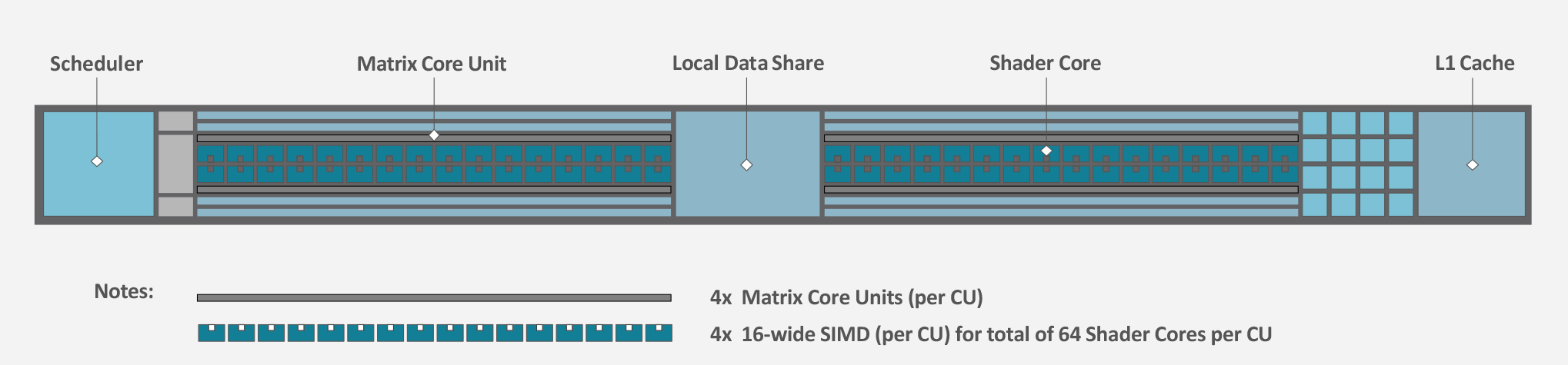
Taking a quick look at an individual CU, we see virtually nothing has changed with respect to organization. CDNA 2 still packs 4 SIMD16 units into a CU, allowing it to process 64 vector instructions per clock. The CUs also contain 4 Matrix Cores each, which are responsible for CDNA 2’s matrix/tensor processing capabilities. All of this, in turn, is paired with a scheduler, a shared L1 cache and load/store units, and the local data share.
What AMD’s diagrams don’t show is that the width of each ALU/shader core within a CU has been doubled. CDNA 2’s ALUs are 64-bit throughout, allowing the architecture to process FP64 operations at full speed. This is twice the rate of MI100, where FP64 operations ran at one-half the rate of FP32 operations.
| AMD GPU Throughput Rates (FLOPS/clock/CU) |
|||||
| CDNA 2 | CDNA (1) | Vega 20 | |||
| FP64 Vector | 128 | 64 | 64 | ||
| FP32 Vector | 128 | 128 | 128 | ||
| Packed FP32 Vector | 256 | N/A | N/A | ||
| FP64 Matrix | 256 | 64 | 64 | ||
| FP32 Matrix | 256 | 256 | 128 | ||
| FP16 Matrix | 1024 | 1024 | 256 | ||
| BF16 Matrix | 1024 | 512 | N/A | ||
| INT8 Matrix | 1024 | 1024 | N/A | ||
This boost to FP64 performance is one of the biggest differences between CDNA 2 and earlier architectures, and it reflects the supercomputer-focused goals of AMD’s design. Even with the rise of machine learning and matrix operations, a lot of data science still requires good ole’ double precision floats processed via SIMDs, and this is exactly what AMD has delivered. AMD has invested heavily in FP64 performance, and as a result MI200 is far, far faster in FP64 vector operations than any other AMD or NVIDIA GPU.
All of this underscores the different directions AMD and NVIDIA have gone; for Ampere, NVIDIA invested almost everything in matrix performance, to the detriment of significantly improving vector performance. AMD on the other hand has gone the other direction; overall throughput per matrix core hasn’t really improved, but vector SIMD performance has.
And it’s not just FP64 performance that AMD’s ALU update affects, either. As a result of the wider ALUs, it’s now possible to take advantage of this hardware with packed instructions. By packing two FP32 instructions in a single float2 vector, each ALU can process two FP32 FMA/FADD/FMUL instructions per clock cycle. Under ideal circumstances, this doubles CDNA 2’s per-CU vector FP32 performance as compared to CDNA (1), for a grand total of over 4x the FP32 performance.
With that said, like all packed instruction formats, packed FP32 isn’t free. Developers and libraries need to be coded to take advantage of it; packed operands need to be adjacent and aligned to even registers. For software being written specifically for the architecture (e.g. Frontier), this is easily enough done, but more portable software will need updated to take this into account. And it’s for that reason that AMD wisely still advertises its FP32 vector performance at full rate (47.9 TFLOPS), rather than assuming the use of packed instructions.
Meanwhile, AMD has also given their Matrix Cores a very similar face-lift. First introduced in CDNA (1), the Matrix Cores are responsible for AMD’s matrix processing. And for CDNA 2, they’ve been expanded to allow full-speed FP64 matrix operations as well, bringing them up to the same 256 FLOPS rate as FP32 matrix operations, a 4x improvement over the old 64 FLOPS/clock/CU rate. Unlike the vector ALUs, however, there are no packed operations or other special cases to take advantage of, so this change doesn’t improve FP32/FP16 performance, which remains at 256 FLOPS and 1024 FLOPS per clock respectively.
AMD has also used this iteration of the CDNA architecture to promote bfloat16 to a full-speed format. Whereas it previously ran at half-speed on CDNA (1), on CDNA 2 it runs at full speed, or 1024 FLOPS/clock/CU.
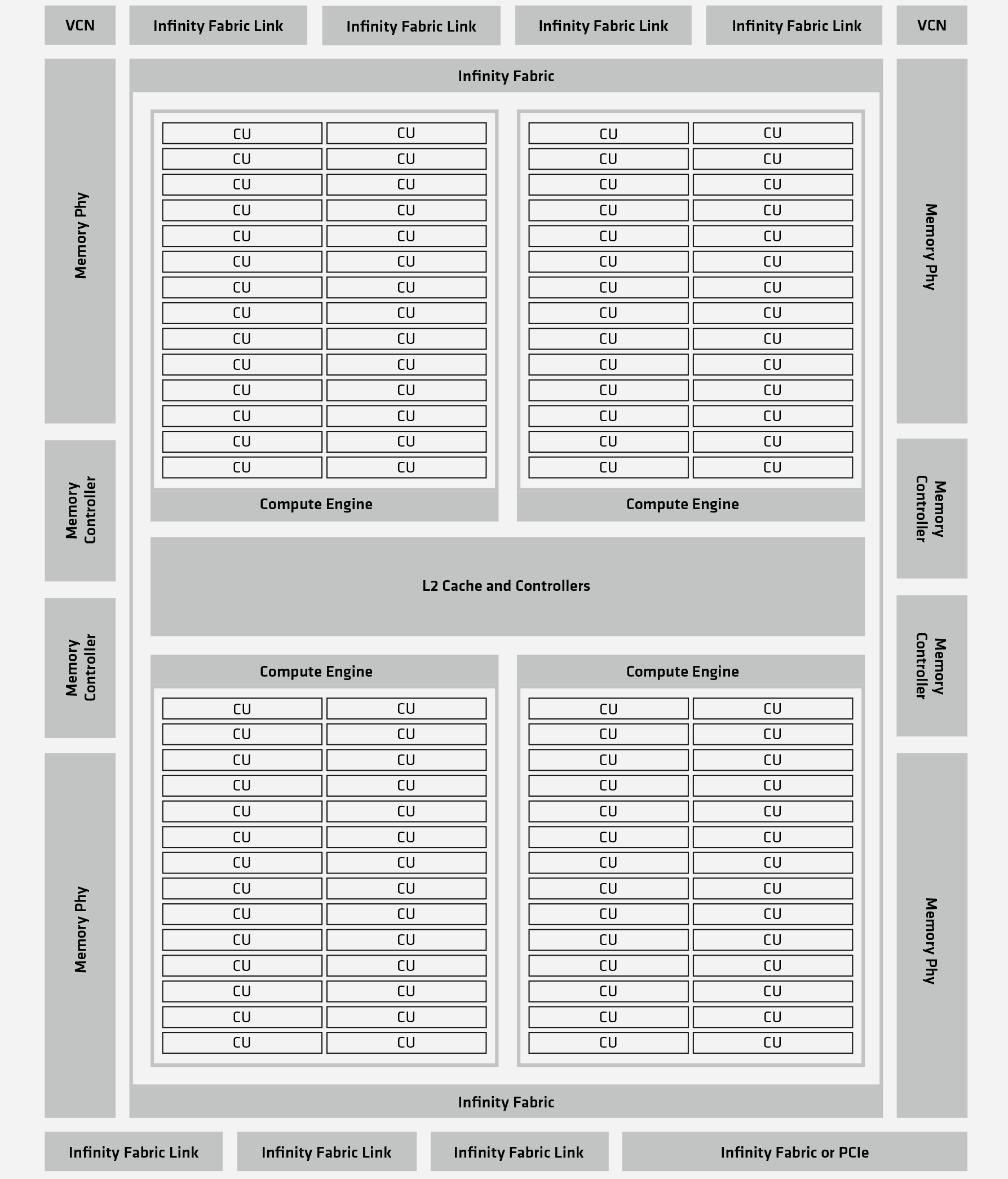
Moving up a level, the general layout of CDNA 2 GPUs is largely unchanged from CDNA (1). The CUs are still divided into 4 Compute Engine groups, and fed by a quartet of Asynchronous Compute Engines (ACEs). As always, AMD obfuscates some of the finer details, but the basic organization is still CDNA as we know it.
Finally, while CDNA 2 is primarily compute-focused, not every last transistor is dedicated to the task. Like its predecessor, CDNA 2 also includes a new version of AMD’s Video Codec Next (VCN) block, which is responsible for video encode and decode acceleration. Judging from AMD’s comments on the matter, this would seem to be included more for decode acceleration than any kind of video encoding tasks, as fast decode capabilities are needed to disassemble photos and videos for use in ML training. This version of the VCN does not support AV1, so the highest format supported for encode/decode is HEVC.
Overall, AMD’s architectural updates for CDNA 2 are relatively modest, but they reflect the kind of changes we’d expect to see for a GPU meant to win a supercomputer contract or three. AMD’s focus on FP64 performance – both vector and matrix – is a good fit for traditional science workloads, and the new packed FP32 instructions should prove useful in those environments as well. Past that, the bulk of AMD’s effort seems to have gone into I/O in order to support the extra 4 IF links, an improvement that should pay off particularly well in the kind of large server clusters and supercomputers AMD is going for.
An EMIB Alternative: Elevated Fanout Bridge 2.5D
Last but not least along our tour of AMD’s Instinct MI200, let’s talk about chip packaging. Besides AMD’s on-die innovations, the MI200 family will also come with an interesting packaging innovation to help connect the GCDs to their respective HBM2E memory stacks. For their new GPUs, AMD is relying on a technology called Elevated Fanout Bridge 2.5D, which takes fanout packaging to the next level by incorporating a small silicon bridge above the substrate itself to connect two dies.
Like all HBM users, AMD has to contend with the memory technology’s unique combination of high speeds and dense trace counts. HBM requires too many traces to be routed through standard substrates, so it needs to be routed through something better: silicon. The end result has been that the first generation of HBM products have used chip-sized silicon interposers, which essentially placed both the HBM stacks and the GPU itself on top of another piece of silicon that has the necessary traces etched into it. Silicon interposers work well enough, but they need to be nearly a big as the entire chip, and that is both expensive and the through-silicon vias (TSVs) make the whole thing less-than-pleasant to assemble.

HBM Circa 2014: Full-size Silicon Interposers
That in turn has led to more recent efforts to focus on installing a much smaller silicon bridge – ideally, something just big enough to cover the HBM-related contacts on both chips. Intel already has a solution to this, EMIB, which places a small bridge die within the substrate. However, besides EMIB being an Intel technology, it’s not without its own drawbacks, so AMD and its fab partners think they can do one better than that. And that one better thing is Elevated Fanout Bridge 2.5D.
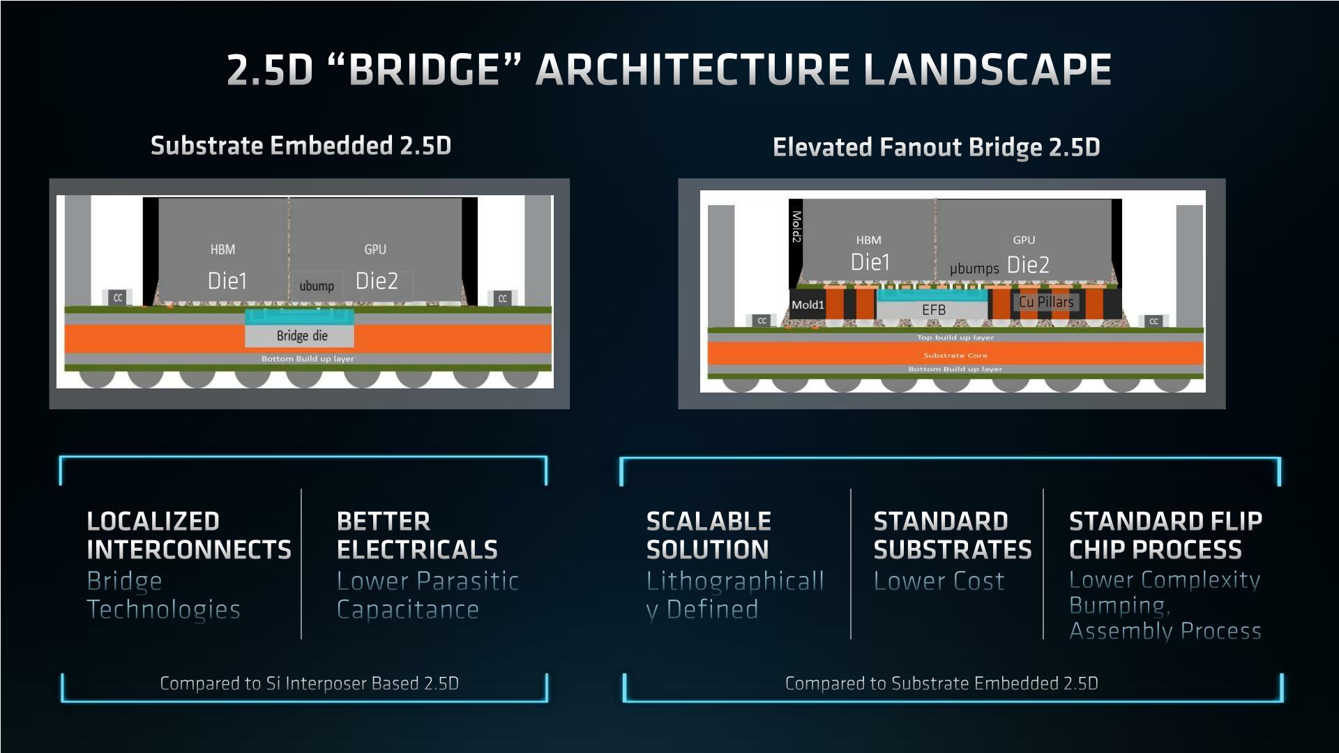
So what makes Elevated Fanout Bridge 2.5D different? In short, EFB builds above the substrate, rather than inside it. In this case, the entire chip pair – the GPU and the HBM stack – are placed on top of a mold with a series of copper pillars in it. The copper pillars allow the coarse-pitched contacts on the chips to make contact with the substrate below in a traditional fashion. Meanwhile, below the high-precision, fine-grained microbumps used for HBM, a silicon bridge is instead placed. The end result is that by raising the HBM and GPU, it creates room to put the small silicon bridge without digging into the substrate.
Compared to a traditional interposer, such as what was used on the MI100, the benefits are obvious: even with the added steps of using EFB, it still avoids having to use a massive and complex silicon interposer. Meanwhile, compared to bridge-in-substrate solutions like EMIB, AMD claims that EFB is both cheaper and less complex. Since everything takes place above the substrate, no special substrates are required, and the resulting assembly process is much closer to traditional flip-chip packaging. AMD also believes that EFB will prove a more scalable solution since it’s largely a lithographic process – a point that’s particularly salient right now given the ongoing substrate bottleneck in chip production.
Overall, EFB looks very similar (if not identical) to TSMC’s InFO-L packaging technology, which was announced back in 2020 and uses an above-substrate bridge. Given the close working relationship between AMD and TSMC, it’s not clear how much of EFB is really an AMD innovation versus them employing InFO-L. But regardless, a more cost-effective means of implementing HBM is a very important step forward for AMD’s GPU team.
MI200 Availability: Frontier First, Everyone Else in Q1’2022
Wrapping things up, while today is the official launch day for the Instinct MI200 family, the new hardware is in fact already shipping. AMD began the first shipments of MI250X parts for the Frontier supercomputer back in Q3 of this year, and they are continuing to ship them in order to fill the US Department of Energy’s order for tens-of-thousands of GPUs.
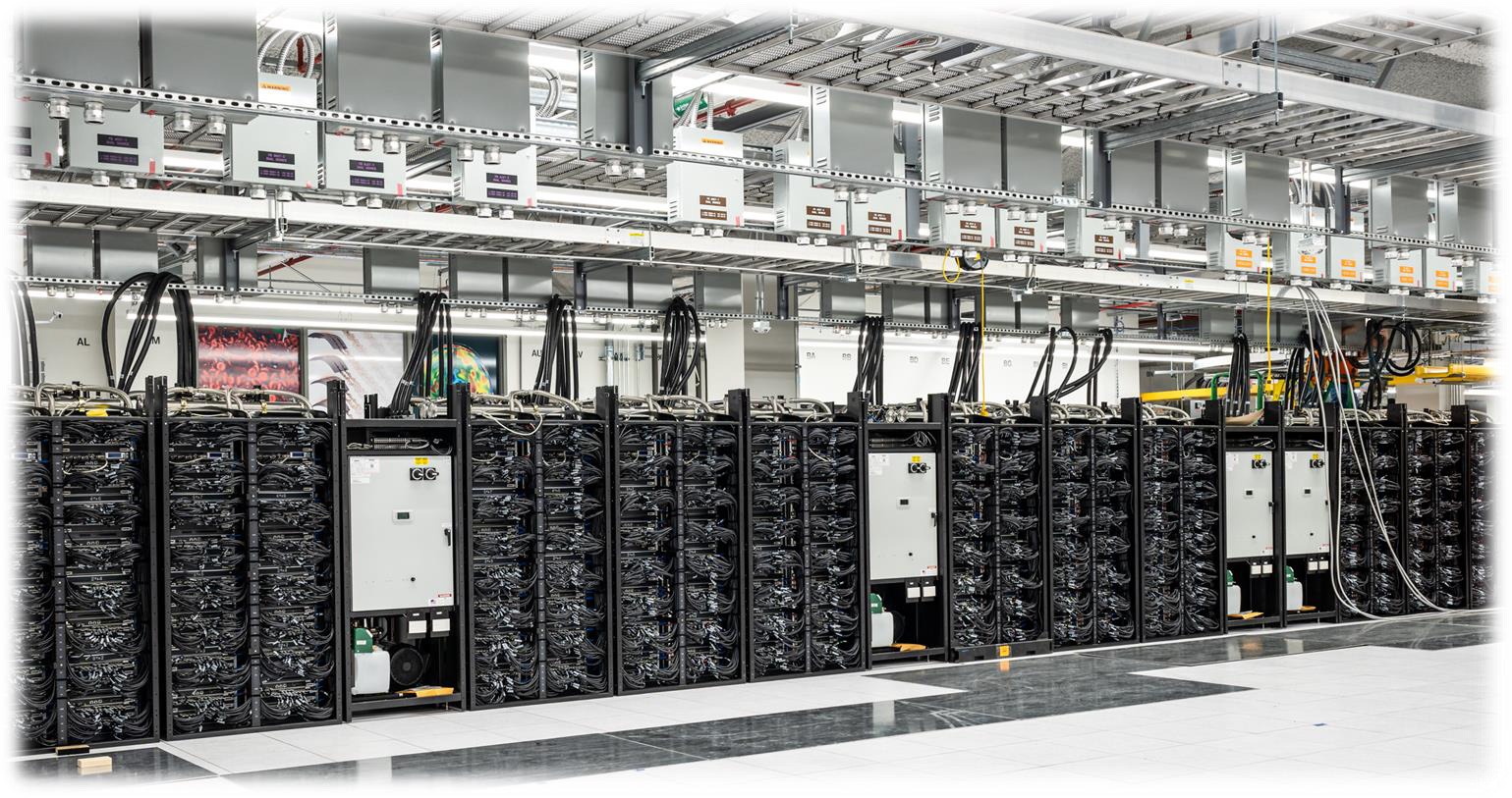
Frontier Supercomputer
Frontier is itself a major success story for AMD, and it’s something AMD is hoping they can use to pivot towards even more success in the server GPU marketplace. With 4 MI250X accelerators in every single node, it’s MI250X that truly underpins the United States’ first exascale computer. And that contract, in turn, has become a major vote of confidence in AMD by the US Department of Energy. As AMD seeks to move into new territory in the server GPU space – and as it seeks to carve out its share of NVIDIA’s lucrative datacenter market – showcasing that their hardware and software stack are ready for wide-scale deployment is critical to winning over customers. All of which is an experience AMD just got through over the last few years on the CPU side of matters.
The MI200 family, in turn, is AMD’s best chance yet to break into the server GPU market in a big way. At the risk of downplaying AMD’s accomplishments here, reaching parity with NVIDIA in form factors and I/O via OAM and Infinity Fabric 3 are going to go a long way towards making their products feature-competitive with the market leader. And AMD’s performance figures, if they pan out in production systems, will help carry them much the rest of the way.
Still, AMD’s competition won’t be sitting still. Intel’s Ponte Vecchio – the heart of the rival Aurora supercomputer – looms close. And market leader NVIDIA has their own cards to play, both figuratively and literally. So there’s ample opportunity for AMD to make gains in the server GPU market over the next cycle, but it’s something they will have to work hard at.
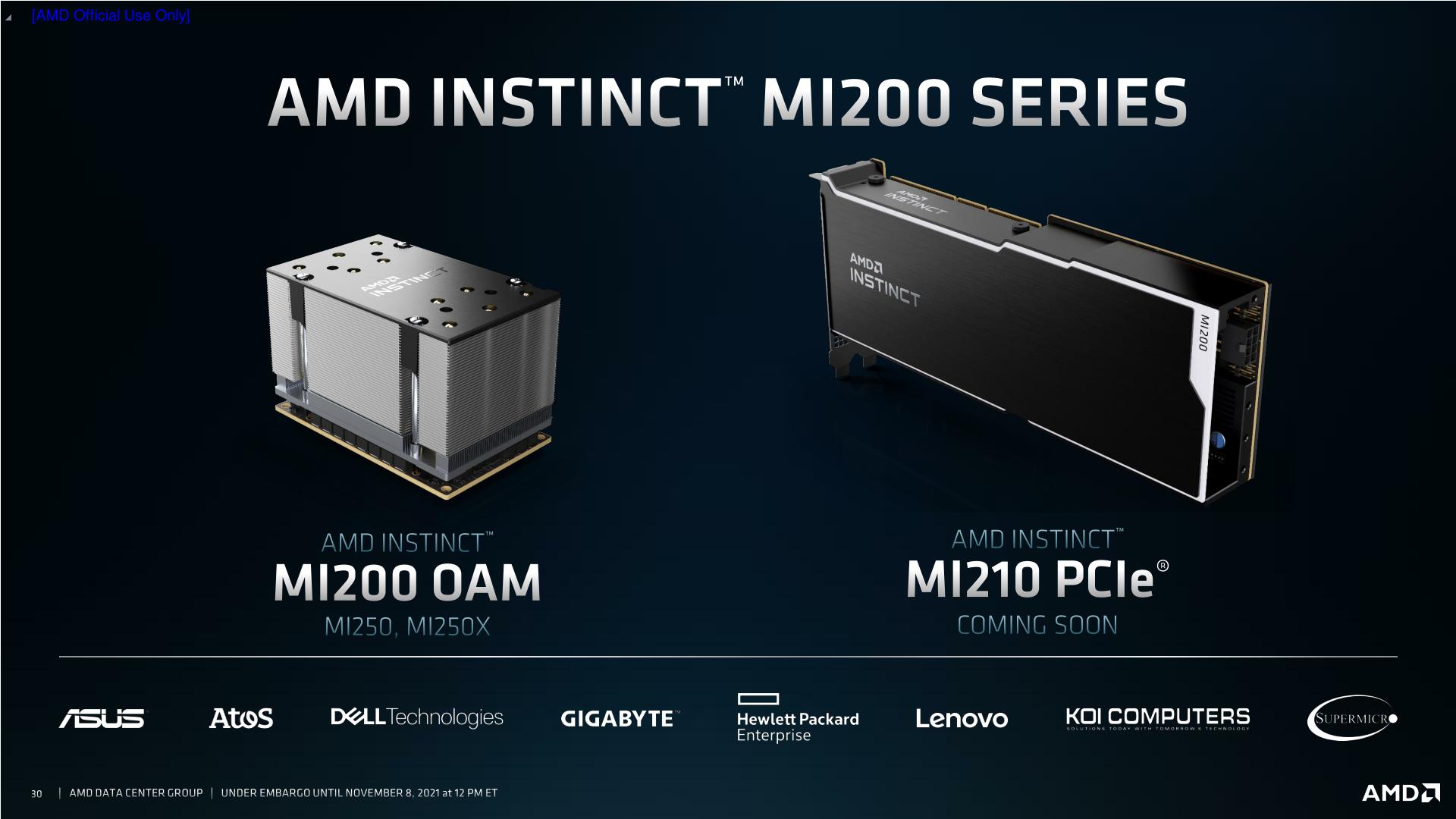
In the meantime, AMD won’t be alone in their journey. After the Frontier order is complete, AMD will be able to begin focusing on ODM and OEM orders, with ODM/OEM availability expected in the first quarter of next year. Many of AMD’s regular partners slated to offer MI200 accelerators in their systems, including Dell, Supermicro, Lenovo, HPE, Gigabyte, and ASUS- and all of whom have been major participants in the success of AMD’s EPYC CPUs as well.


61 Comments
View All Comments
xhris4747 - Tuesday, November 9, 2021 - link
ROCm officially supports AMD GPUs that use following chips:GFX8 GPUs
“Fiji” chips, such as on the AMD Radeon R9 Fury X and Radeon Instinct MI8
“Polaris 10” chips, such as on the AMD Radeon RX 580 and Radeon Instinct MI6
“Polaris 11” chips, such as on the AMD Radeon RX 570 and Radeon Pro WX 4100
“Polaris 12” chips, such as on the AMD Radeon RX 550 and Radeon RX 540
GFX9 GPUs
“Vega 10” chips, such as on the AMD Radeon RX Vega 64 and Radeon Instinct MI25
“Vega 7nm” chips, such as on the Radeon Instinct MI50, Radeon Instinct MI60 or AMD Radeon VII
mode_13h - Wednesday, November 10, 2021 - link
But still no RDNA or RDNA2? That's a problem.Spunjji - Wednesday, November 10, 2021 - link
They split the compute and gaming architectures after RDNA, so I'm not sure how much use it would be to support that when it's diverging from the CDNA architectures they're selling into servers.mode_13h - Wednesday, November 10, 2021 - link
Tell Nvidia that. They did basically the same thing, as far as bifurcating their product lines, but I guess they should've dropped CUDA on their gaming cards?You sound just as clueless as AMD.
mode_13h - Wednesday, November 10, 2021 - link
A big thing that Nvidia got right about CUDA was supporting it across virtually their entire product stack. From the small Jetson Nano platform, up through nearly all of their consumer GPUs, and obviously including their workstation & datacenter products.Students could then buy a GPU to use for coursework, whether deep learning, computer vision, or perhaps even scientific computing, and get double duty out of it as a gaming card. These same students are creating the next generation of apps, libraries, and frameworks. So, it's very short-term focused for AMD to prioritize HIP and HPC projects above support of their compute stack on all their gaming GPUs.
Helmery - Monday, November 8, 2021 - link
"to not just recapture lost glory, but to rise higher than the company ever has before"... and they did it!Rise, Zen, Ryzen... Epyc Lisa Su and Lisa team!
hd-2 - Monday, November 8, 2021 - link
Tesla D1 (on N7) claimed 362 TFLOPs of BF16 and 22.6 TFLOPs of FP32 (vector?) at 400W, with 1.1ExaFLOS of FP16/CFP8 on 3000 D1 chips (354 nodes each). Still hard to compare since some of the other metrics aren't listed for both and there was never a deep dive into D1 here at AT afaik.blanarahul - Monday, November 8, 2021 - link
In the consumer space, GA102 already had 28.3 billion transistors @ 628 sq mm. I don't expect Nvidia to create a dual die graphics card just yet. Makes me wonder how big the RTX 4090 will be and if it will use EFB/InFO-L attached HBM memory.mmschira - Monday, November 8, 2021 - link
The compute acceleration space is getting really interesting, but the fragmentation of this space is a real headache and I can't see anybody trying to fight this.Nvida requires CUDA,
Apple requires Metal
AMD?
Intel?
What are their programing interfaces?
Kevin G - Tuesday, November 9, 2021 - link
Intel had One API as a proprietary solution that spans their product portfolio (including some dedicated AI accelerators and FPGA products).AMD was a big proponent of OpenCL back in the day. Intel and nVidia also support OpenCL as an interoperable solution though they favor their own proprietary solutions.