TSMC's 3nm Journey: Slow Ramp, Huge Investments, Big Future
by Anton Shilov on January 17, 2023 9:00 AM EST- Posted in
- Semiconductors
- TSMC
- 3nm
- N3
Last week, TSMC issued their Q4 and full-year 2022 earnings reports for the company. Besides confirming that TSMC was closing out a very busy, very profitable year for the world's top chip fab – booking almost $34 billion in net income for the year – the end-of-year report from the company has also given us a fresh update on the state of TSMC's various fab projects.
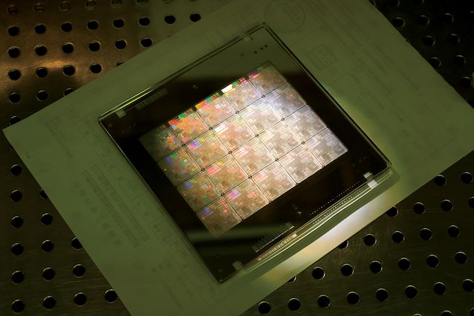
The big news coming out of TSMC for Q4'22 is that TSMC has initiated high volume manufacturing of chips on its N3 (3nm-class) fabrication technology. The ramp of this node will be rather slow initially due to high design costs and the complexities of the first N3B implementation of the node, so the world's largest foundry does not expect it to be a significant contributor to its revenue in 2023. Yet, the firm will invest tens of billions of dollars in expanding its N3-capable manufacturing capacity as eventually N3 is expected to become a popular long-lasting family of production nodes for TSMC.
Slow Ramp Initially
"Our N3 has successfully entered volume production in late fourth quarter last year as planned, with good yield," said C. C. Wei, chief executive of TSMC. "We expect a smooth ramp in 2023 driven by both HPC and smartphone applications. As our customers' demand for N3 exceeds our ability to supply, we expect the N3 to be fully utilized in 2023."
Keeping in mind that TSMC's capital expenditures in 2021 and 2022 were focused mostly on expanding its N5 (5nm-class) manufacturing capacities, it is not surprising that the company's N3-capable capacity is modest. Meanwhile, TSMC does not expect N3 to account for any sizable share of its revenue before Q3.
In fact, the No. 1 foundry expects N3 nodes (which include both baseline N3 and relaxed N3E that is set to enter HVM in the second half of 2023) to account for maybe 4% - 6% of the company's wafer revenue in 2023. And yet this would exceed the contribution of N5 in its first two quarters of HVM in 2020 (which was about $3.5 billion).
"We expect [sizable N3 revenue contribution] to start in third quarter 2023 and N3 will contribute mid-single-digit percentage of our total wafer revenue in 2023," said Wei. "We expect the N3 revenue in 2023 to be higher than N5 revenue in its first year in 2020."
Many analysts believe that the baseline N3 (also known as N3B) will be used by Apple either exclusively or almost exclusively, which is TSMC's largest customer that is willing to adopt leading-edge nodes ahead of all other companies, despite high initial costs. If this assumption is correct and Apple is indeed the primary customer to use baseline N3, then it is noteworthy that TSMC mentions both smartphone and HPC (a vague term that TSMC uses to describe virtually all ASICs, CPUs, GPUs, SoCs, and FPGAs not aimed at automotive, communications, and smartphones) applications in conjunction with N3 in 2023.
N3E Coming in the Second Half
One of the reasons why many companies are waiting for TSMC's relaxed N3E technology (which is entering HVM in the second half of 2023, according to TSMC) is the higher performance and power improvements, as well as even more aggressive logic scaling. Another is that the process will offer lower costs, albeit at the cost of a lack of SRAM scaling compared to N5, according to analysts from China Renaissance.
"N3E, with six fewer EUV layers than the baseline N3, promises simpler process complexity, intrinsic cost and manufacturing cycle time, albeit with less density gain," Szeho Ng, an analyst with China Renaissance, wrote in a note to clients this week.
| Advertised PPA Improvements of New Process Technologies Data announced during conference calls, events, press briefings and press releases |
|||
| TSMC | |||
| N3 vs N5 |
N3E vs N5 |
||
| Power | -25-30% | -34% | |
| Performance | +10-15% | +18% | |
| Logic Area Reduction* % Logic Density* |
0.58x -42% 1.7x |
0.625x -37.5% 1.6x |
|
| SRAM Cell Size | 0.0199µm² (-5% vs N5) | 0.021µm² (same as N5) | |
| Volume Manufacturing |
Late 2022 | H2 2023 | |
Ho says that TSMC's original N3 features up to 25 EUV layers and can apply multi-patterning for some of them for additional density. By contract, N3E supports up to 19 EUV layers and only uses single-patterning EUV, which reduces complexity, but also means lower density.
"Clients' interest in the optimized N3E (post the baseline N3B ramp-up, which is largely limited to Apple) is high, embracing compute-intensive applications in HPC (AMD, Intel), mobile (Qualcomm, Mediatek) and ASICs (Broadcom, Marvell)," wrote Ho.
It looks like N3E will indeed be TSMC's main 3nm-class working horse before N3P, N3S, and N3X arrive later on.
Tens of Billions on N3
While TSMC's 3nm-class nodes are going to earn the company a little more than $4 billion in 2023, the company will spend tens of billions of dollars expanding its fab capacity to produce chips on various N3 nodes. This year the company's capital expenditures are guided to be between $32 billion - $36 billion. 70% of that sum will be used on advanced process technologies (N7 and below), which includes N3-capable capacity in Taiwan, as well as equipment for Fab 21 in Arizona (N4, N5 nodes). Meanwhile 20% will be used for fabs producing chips on specialty technologies (which essentially means a variety of 28nm-class processes), and 10% will be spent on things like advanced packaging and mask production.
Spending at least $22 billion on N3 and N5 capacity indicates that TSMC is confident on the demand for these nodes. And there is a good reason for that: the N3 family of process technologies is set to be TSMC's last FinFET-based family of production nodes for complex high-performance chips. The company's N2 (2nm-class) manufacturing process will rely on nanosheet-based gate-all-around field-effect transistors (GAAFETs). In fact, analyst Szeho Ng from China Renaissance believes that a significant share of this year's CapEx set for advanced technologies will be spent on N3 capacity, setting the ground for roll-out of N3E, N3P, N3X, and N3S. Since N3-capable fabs can also produce chips on N5 processes, TSMC will be able to use this capacity where there will be significant demand for N5-based chips as well.
"TSMC guided 2023 CapEx at $32-36bn (2022: US$36.3bn), with its expansion focused on N3 in Fab 18 (Tainan)," the analyst wrote in a note to clients.
Since TSMC's N2 process technology will only ramp starting in 2026, N3 will indeed be a long lasting node for the company. Furthermore, since it will be the last FinFET-based node for advanced chips, it will be used for many years to come as not all applications will need GAAFETs.


30 Comments
View All Comments
whatthe123 - Wednesday, January 18, 2023 - link
The delays are due to TSMC struggling with their original 3nm target. That's why there is now a new, less dense 3nm node that everyone will be using instead and why they don't expect much revenue out of the current n3 node. If the original N3 was ready for high volume Apple would've probably jumped on it to stamp out the competition like they did with the first run of 5nm.webdoctors - Tuesday, January 17, 2023 - link
Amazing stuff. being on 3nm in 2023. I remember working on chip designs on 130nm and 90nm back in 2003 thinking how incredible that was. We've made crazy strides in 20 years. Wonder what process we'll be on in 10 or 20 years.haukionkannel - Wednesday, January 18, 2023 - link
Well 130nm and 90 nm were allmort 130nm and 90nm while 3nm is something like 30 to 40nm in reality so the advancement is not as high as sales man claims…FreckledTrout - Friday, January 20, 2023 - link
Things get even wonkier with TSMC's 2nm as they switch to GAA so there is even more of the transistor in 3 dimensions. The nm terms are more marketing than anything else these days which Intel acknowledged with their new names.Threska - Friday, January 20, 2023 - link
Problems problems.https://www.tomshardware.com/news/materials-breakt...
mattbe - Tuesday, January 24, 2023 - link
If this is what you are arguing, a 130nm has a gate length of around 130nm while a 3nm chip has a gate length of about 16-18nm. The 30-40nm is pulled out of your ass. If you are talking about the pitch, then at the 130nm node, the pitch wasn't 130nm either...sharath.naik - Wednesday, January 18, 2023 - link
Its close to reaching its limits. at 3nm my guess is its just 10-20 atoms. could they go to 1nm? it will be remarkable if they do. but you see how close they are to the limits.escksu - Wednesday, January 18, 2023 - link
Oh no, it's not 3nm. "3nm" or "5nm" today is no longer a true indication of transistor size. Actual size is around 30nm. It's more to do with marketing instead.Back then when we had only planar transistor, yes. But today we have finfet, gaafet etc so the size is just more of an estimation of planar equivalent with lots of assumptions made.
There is no standard of how you define 3nm or 5nm. It entirely up to the company.
mattbe - Tuesday, January 24, 2023 - link
"There is no standard for defining 3nm or 5nm. It is entirely up to the company."There is some semblance ot standard as established by IMEC. It would be bad for the company's image if it's too far off IMEC's expected specs for that node...
ABR - Thursday, January 19, 2023 - link
They don't even try to say it's 3nm any more. It's "N3". Of course they want you to make the association, but that's on you then.