ASUS P5B-E: P965 stepping C1 versus C2, Round One
by Gary Key on October 4, 2006 9:00 AM EST- Posted in
- CPUs
Overclocking
Our BIOS settings were fairly conservative as we left the memory settings at Auto. We tried fine tuning each of ten different memory options but in the end the board responded better over the 485FSB level with memory set at Auto timings. We changed our voltage and other settings to 2.10V RAM, 1.450V FSB Termination, 103 MHz PCI Express, PCI fixed at 33.33MHz, DRAM Frequency at 1:1, Spread Spectrum disabled, Static Read Control disabled, and all power conservation settings disabled. Dialing in the proper CPU voltage was tricky at times due to the voltage droop on this board. In our final settings we found 1.5250V ended up being around 1.4875V under load with 1.5000V dropping to 1.4625V.
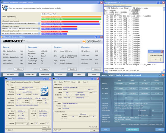
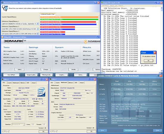
We were amazed by our overclocking results on this board with either MCH stepping as we figured the lack of MCH voltage adjustability and memory voltages not exceeding 2.10V would have hampered our clocks to the mid-400 FSB level. Like other ASUS boards, we had to gradually increase the FSB speeds while adjusting CPU voltages and memory settings in order to reach this level. Our retail E6300 was able to boot into Windows XP at 7x521 but we consistently had benchmark failures until we backed off to 7x515 on the C1 stepping and 7x514 on the C2 stepping. With our component choices these standard overclock levels were solid for 24/7 operation. We are currently testing the overclocking capability of our E6600 and E6400 processors for the next article update. We were not able to exceed the 525MHz FSB level when dropping the CPU multiplier to 6. We could post at 6x533 with either stepping but once again the stable limit was at 6x525. We see this limitation as a combination of not having enough MCH voltage and the inability to increase our memory voltage past 2.10V. In the end, both MCH steppings overclocked in the same manner although we found the memory and 3DMark06 scores to slightly favor the C2 stepping even with the C1 stepping system having a slightly higher overclock, maybe our Intel engineer was correct about the minor memory tweaks.
Considering the BIOS limitations we have with the memory and MCH voltages it is impossible to tell if the C2 stepping would really overclock better on this board or not; we do know for a fact that our C1 seems to be every bit the equal to our C2 stepping. This is exactly what the motherboard suppliers have been telling us and why they will not be changing the board designations when the switchover to C2 occurs. The majority of the suppliers we contacted expect this switchover to be complete by the end of October. We expect the current overclocking capability will change when a supplier introduces a new board or BIOS design that takes additional advantage of the P965 chipset. However, we have been informed that even in this case the two steppings are almost identical in performance with the board layout, BIOS, and components being the most critical areas in improving overclocking. After testing two other C2 stepping motherboards we found a difference of 12 FSB between identical boards so the luck of the draw in getting a good MCH is just as important as getting an overclock friendly CPU.
| Asus P5B-E Overclocking Testbed |
|
| Processor: | Intel Core 2 Duo E6300 Dual Core, 1.86GHz, 2MB Unified Cache 1066FSB, 7x Multiplier |
| CPU Voltage: | 1.5250V (default 1.3250V) |
| Cooling: | Scythe Infinity Air Cooling |
| Power Supply: | OCZ GameXStream 700W |
| Memory: | Corsair Twin2X2048-PC2-6400C3 (2x1GB), 2.10V (Micron Memory Chips) |
| Video Cards: | 1 x MSI X1950XTX |
| Hard Drive: | Seagate 320GB 7200RPM SATA2 16MB Buffer |
| Case: | Cooler Master CM Stacker 830 |
| Maximum CPU OC: (Standard Ratio) |
515x7 (4-4-4-12, 1:1), CPU 1.5250V C1 Stepping - 3610MHz (+93%) |
| 514x7 (4-4-4-12, 1:1), CPU 1.5250V C2 Stepping - 3602MHz (+93%) |
|
| Maximum FSB OC: (Lowest Ratio) |
525x6 (5-4-5-12, 1:1), CPU 1.5000V C1 Stepping - 3148MHz (+97%) |
| 525x6 (5-4-5-12, 1:1), CPU 1.5000V C2 Stepping - 3148MHz (+97%) |
|
Our BIOS settings were fairly conservative as we left the memory settings at Auto. We tried fine tuning each of ten different memory options but in the end the board responded better over the 485FSB level with memory set at Auto timings. We changed our voltage and other settings to 2.10V RAM, 1.450V FSB Termination, 103 MHz PCI Express, PCI fixed at 33.33MHz, DRAM Frequency at 1:1, Spread Spectrum disabled, Static Read Control disabled, and all power conservation settings disabled. Dialing in the proper CPU voltage was tricky at times due to the voltage droop on this board. In our final settings we found 1.5250V ended up being around 1.4875V under load with 1.5000V dropping to 1.4625V.
 |
| Click to enlarge |
 |
| Click to enlarge |
We were amazed by our overclocking results on this board with either MCH stepping as we figured the lack of MCH voltage adjustability and memory voltages not exceeding 2.10V would have hampered our clocks to the mid-400 FSB level. Like other ASUS boards, we had to gradually increase the FSB speeds while adjusting CPU voltages and memory settings in order to reach this level. Our retail E6300 was able to boot into Windows XP at 7x521 but we consistently had benchmark failures until we backed off to 7x515 on the C1 stepping and 7x514 on the C2 stepping. With our component choices these standard overclock levels were solid for 24/7 operation. We are currently testing the overclocking capability of our E6600 and E6400 processors for the next article update. We were not able to exceed the 525MHz FSB level when dropping the CPU multiplier to 6. We could post at 6x533 with either stepping but once again the stable limit was at 6x525. We see this limitation as a combination of not having enough MCH voltage and the inability to increase our memory voltage past 2.10V. In the end, both MCH steppings overclocked in the same manner although we found the memory and 3DMark06 scores to slightly favor the C2 stepping even with the C1 stepping system having a slightly higher overclock, maybe our Intel engineer was correct about the minor memory tweaks.
Considering the BIOS limitations we have with the memory and MCH voltages it is impossible to tell if the C2 stepping would really overclock better on this board or not; we do know for a fact that our C1 seems to be every bit the equal to our C2 stepping. This is exactly what the motherboard suppliers have been telling us and why they will not be changing the board designations when the switchover to C2 occurs. The majority of the suppliers we contacted expect this switchover to be complete by the end of October. We expect the current overclocking capability will change when a supplier introduces a new board or BIOS design that takes additional advantage of the P965 chipset. However, we have been informed that even in this case the two steppings are almost identical in performance with the board layout, BIOS, and components being the most critical areas in improving overclocking. After testing two other C2 stepping motherboards we found a difference of 12 FSB between identical boards so the luck of the draw in getting a good MCH is just as important as getting an overclock friendly CPU.


27 Comments
View All Comments
Gary Key - Wednesday, October 4, 2006 - link
The highest we could get while keeping the memory timings tight was 485FSB, that level required 2.10V on the memory and 1.4625V on the CPU. Anything over 485FSB, we just let the board handle the memory timings automatically, probably could have decreased tRAS to 10.xsilver - Wednesday, October 4, 2006 - link
ok,then how high can it go on default voltages? northbridge,dram,cpu
thanks
Ecmaster76 - Wednesday, October 4, 2006 - link
C1 -> C2 implies a very minor change.Conventionally a major reviosion comes with a new letter designation like C1 -> D#
Plus performance improvements of the magnitude apparently rumored would not be sold as the same chipset. Instead it would probably be marketed as a new product and perhaps even released with a new socket or voltage regulation standard to make upgrading even more fun.
Tujan - Wednesday, October 4, 2006 - link
Found myself just getting out of the middrift to browse ASUS for that notorious AMD ATI motherboard wich shouldhave been out in September.Of course I couldn't keep myself from looking at the 775 Intel MBs from ASUS. There is was an ASUS P5B. 1 PCIexpress,and 3PCI . Passive cooling,and an eSata to go with it.
Then alas I still had to find somebody who had something using a 'Core-Duo for sale. To use it. The same story,just enough in a review and nothing on the retail,or you could find something in some foreign country..perhaps.
Yes,there IS a Asus P5B for sale.Yes,it IS an ASUS P5B-E !!! No,..im not going to tell you where. Nananana no,no...(snickers).
Seriously,the Asus P5B fits right there between the other single PCI-e 965 motherboards I have read reviewed on Anandtechs website. I count around 4 of them at the present time. But I keep reading. There is a Foxconn board out there somewhere with the same type of derivitive numbering. Still different specs.and performer however.
Cant really say too much now can we. Dont want to upset the 975x boys now.
ASUS P5B motherboard looks like a "nice"motherboard.
rawr1234 - Thursday, October 5, 2006 - link
You guys didnt test Rev 1.02G ... only 1.01G, rev 1.02G is soposed to be able to change the volt on ram up to 2.45v and it comes with C2Gary Key - Thursday, October 5, 2006 - link
We have another 1.02G board coming, the 1.01G boards actually clocked better. You will see the 1.02G results late next week.JarredWalton - Thursday, October 5, 2006 - link
That was sort of the point - this is an "apples to apples" comparison of C1 and C2 on a motherboard that will ship with both revisions. Testing a C2-only board and drawing conclusions that C2 is better isn't fair - maybe it's just the board that's better. So basically, any improvements over C1 boards judging by this article are going to be largely due to the improved motherboard/BIOS designs and not the chipset revision.