Crucial MX100 (256GB & 512GB) Review
by Kristian Vättö on June 2, 2014 3:00 PM ESTIMFT's 16nm NAND
As I mentioned in the Plextor M6S & M6M review a couple of months ago, IMFT is doing something differently with their 20nm NAND. Let's see what it looks like:
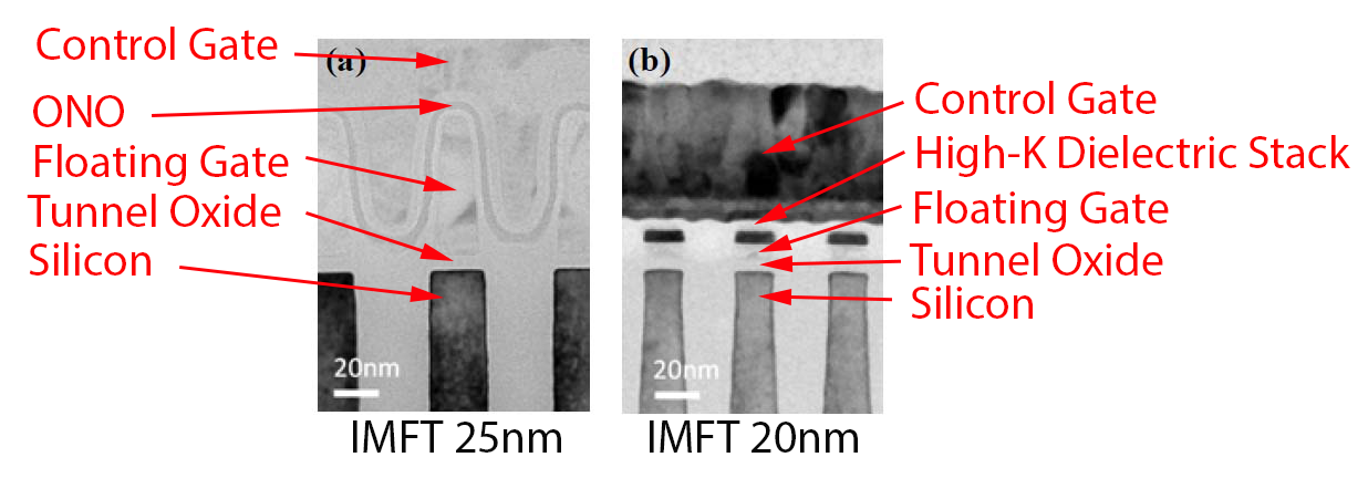
That is what a cross-section of IMFT's 20nm NAND looks like in comparison to the 25nm node. There's quite a big difference. The 25nm node still used the traditional wrapping technology where the wordline (i.e. control gate) wrapped around every floating gate. However, the issue with this approach is its limited scalability. In addition to the wordline, the oxide-nitride-oxide layer (i.e. ONO) must be wrapped around every floating gate as well to insulate the floating gate because otherwise the electrons would be free to escape. And here lies the problem: the ONO layer cannot really be scaled any further without jeopardizing reliability because if it's too thin, it will not be able to reliably insulate the cell.
Furthermore, the reason why the wordline must be wrapped around each floating gate is to build enough capacitance between the control and floating gates as otherwise programming efficiency is lost. Remember that the way NAND works is basically fighting against the fundamental laws of physics because you are shooting electrons through an insulator, so the capacitance is crucial for quick and efficient programming.
If you can't scale the ONO layer, what do you do? Simply, you get rid of it and replace it with something better. The better in this case is a stack of high-K dielectrics. If you are familiar with Intel's CPU architectures, you may be familiar with the term as Intel introduced it to their CPUs with their 45nm process node. The high-K term refers to high dielectric constant, called K. The higher the constant K is, the higher the capacitance when the material is used as a dielectric. Obviously, high-K means that the constant is high, so the capacitance is also high.
All of the parts are now falling into place, right? Because the high-K dielectric stack has a much higher K value than the ONO layer, it's able to provide the same capacitance without the need for wrapping. As a result the technology is more scalable because the ONO wrap is no longer the obstacle.
IMFT introduced the high-K technology in their 20nm NAND and they are using the same technology in the brand new 16nm process. Unfortunately IMFT wouldn't disclose any details of their 16nm NAND (not even the die size) but this is most likely a symmetrical (i.e. 16nm*16nm) design as the use of high-K dielectrics allows scaling in both X and Y axes without major sacrifices in endurance or reliability. As a result the cell size is likely the smallest in the industry -- even though Toshiba's/SanDisk's NAND is officially called 15nm, they have not given any indication of the use of high-K dielectrics, which means the design is likely asymmetrical (e.g. 15nm*19nm) like their previous designs.
I'm guessing IMFT has a pretty significant lead in the high-K development given that Intel (the other half of IMFT) has been using them in their CPUs for years now. We'll find out more about the new NAND lithographies from every manufacturer as TechInsights and other companies specialized in semiconductor analysis are able to x-ray and analyze them.
The State of 3D NAND
If you've been following the SSD and NAND market for a while, it's likely that you have heard of 3D NAND. Scaling of standard NAND is starting to hit the laws of physics and it's getting tougher and tougher to shrink the cell size without driving into serious reliability and endurance issues. The cell size is simply getting so small that it can only hold a dozen or so electrons, which means that even a loss of one or two electrons through leakage/trapping can lead to a big enough change in the floating gate voltage that the cell becomes unreadable (i.e. it won't return the correct outcome).
This is where 3D NAND comes in. It puts a reset to the traditional planar scaling by stacking cells vertically. Now, just to be clear, this isn't the same as stacking several 2D NAND dies on top of each other, not at all. 3D NAND does the stacking at the wafer level, which leads to the actual die having multiple layers of cells (hence the 3D moniker). All NAND manufacturers are developing their own 3D NAND technologies and the approaches are all a bit different. Anand covered Samsung's technology in detail in our V-NAND announcement article but I'll save the analysis of the other manufacturers' technologies for a future article. Today we'll just look at the 3D NAND schedule for every manufacturer.
| IMFT | Samsung | Toshiba/SanDisk | SK Hynix |
| Q4'14 | Q3'13 | H1'16 | H2'14 |
Currently Samsung is the only company that has 3D NAND in mass production. Samsung has been producing their 128Gbit 24-layer 3D NAND in their Korean fabs since last August and just a few days ago they announced their second generation 3D NAND (or V-NAND as Samsung calls it). This is a 32-layer part with a die capacity of 86Gbit, so it looks like Samsung has cut the die size in half compared to their first gen V-NAND with the added layers providing the increase in density (64Gbit*1.33 is ~85Gbit). From what I have heard Samsung is using the same manufacturing equipment for their second gen V-NAND, so the odd capacity point makes sense because it's probably easier to optimize the controller for 86Gbit die instead of ~170Gbit, especially when dealing with low capacity drives/devices.
Furthermore, Samsung announced a while ago that their new facility in Xi'an, China has started the production of 3D NAND. The new fab isn't fully completed yet but Samsung expects it to be completed by the end of this year; regardless, it's clear that Samsung is leading the transition to 3D NAND. We will probably see 3D NAND make its first appearance in client-class SSDs this year because along with the second gen V-NAND announcement, Samsung also announced that they are already shipping 3D NAND SSDs to PC OEMs. However, I wouldn't totally rule out the possibility of yet another 2D NAND die shrink before Samsung moves to 3D NAND full time as from what I have heard, 3D NAND isn't currently very economical for Samsung and the price and characteristics make it more suitable for the enterprise market.
IMFT currently has samples of their 3D NAND but they are keeping everything in-house to make sure their competitors don't get their hands on them. Mass production is expected by the end of this year, although IMFT is making it clear that their 3D NAND won't replace 2D NAND anytime soon. Instead IMFT is developing a 256Gbit version of their 16nm NAND to remain price competitive and I've heard they are even working on a 10nm to 15nm process node. The usage of high-K gate dielectric certainly helps to scale traditional NAND even further but I guess it's ultimately up to how the 3D NAND production starts. If yields are good and the design is economical enough, there may not be a need for another 2D NAND die shrink, but we will probably hear more later this year.
SK Hynix is also planning mass production of their 3D NAND later this year. Similar to IMFT, SK Hynix believes that 2D and 3D NAND will co-exist for at least a couple of years until the challenges of manufacturing 3D NAND are solved. SK Hynix is currently entering mass production of their 16nm NAND, although it's not certain whether this is a symmetrical (16nm*16nm) design or whether it uses high-K dielectrics.
Last but not least, we have the Toshiba/SanDisk joint-venture. Their 3D NAND won't see mass production until early 2016, which is at least a year later than others. Toshiba and SanDisk believe that their 2D NAND is more cost efficient at the moment and thus see no need to move to 3D NAND yet. Their just announced 15nm NAND will be their last 2D NAND node but we probably won't see it in products until late this year or early next year, so that will cover the market for about a year before being replaced by 3D NAND.
All in all, the state of the NAND industry is certainly interesting. A lot will be happening in the next few years, though 3D NAND won't revolutionize the industry. (ReRAM and MRAM, on the other hand, may). I'm confident that 2D NAND will continue to be the go-to form of non-volatile memory for the mainstream market for the next two years or so and 3D NAND will be geared more towards enterprise, but we will see how things turn out.
And with that out of the way, let's move on to the performance testing of the Crucial MX100.


50 Comments
View All Comments
s44 - Tuesday, June 3, 2014 - link
Space will be the same, they're just advertised differently. But the Crucial idles at much lower power than the Seagate, so I'd consider switching to save battery life.tobho - Tuesday, June 3, 2014 - link
Some serious question over here: is this drive a real competitor to the Sammys Evo or even Pro SSDs? I was planning on buying the 256Pro but the Crucial seems to perform better in a lot of tasks. I cannot really differentiate much but the price: 256Pro = 512MX100hojnikb - Tuesday, June 3, 2014 - link
Just get MX100. For the price, its a steal..rvb3n - Tuesday, June 3, 2014 - link
Hi, can someone give me a suggestion for a pro SSD for a laptop with about 500 GB? Is the Samsung 840 Pro still the king (price/performance)?blackrain - Tuesday, June 3, 2014 - link
Looking forward to the Bench being updated with the Crucial MX100 line:http://www.anandtech.com/bench/SSD/65
blackrain - Tuesday, June 3, 2014 - link
I wonder how my Samsung 830 128GB compares to the MX100 128GB? Again, looking forward to the Bench being updated with the MX100 line.Kristian Vättö - Wednesday, June 4, 2014 - link
They were there, but just hidden so we wouldn't break NDA. Should be visible now :)rahuldesai1987 - Tuesday, June 3, 2014 - link
A 256Gbit die should enable a $300 1TB and $600 2TB drive, 6 months down the line. Hope we see a TLC Samsung 850EVO soon, at even cheaper prices.sequoia464 - Tuesday, June 3, 2014 - link
Killer prices on these already,, picked up a 256 GB drive this morning for ~$90 delivered.Oyster - Tuesday, June 3, 2014 - link
For those that are interested, looks like these are on a fire sale.512GB $200, 256GB $100, 128GB $70 AC
http://slickdeals.net/f/6972254-crucial-mx100-soli...