An Introduction to Semiconductor Physics, Technology, and Industry
by Joshua Ho on October 9, 2014 3:00 PM EST- Posted in
- Semiconductors
- CMOS
- Physics
- Industry
- Technology
Transistors
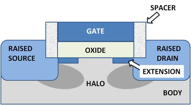
MOSFET Junction Structure / Brews Ohare / CC BY SA
The next inevitable question is how to make a transistor. While there are many other methods of making transistors, it’s best to focus on the one that is used in modern computer chips, namely the metal-oxide-semiconductor field-effect-transistor or MOSFET.
This is a relatively simple design, although there’s a great deal of complexity in its implementation. This type of transistor has four terminals: source, gate, drain, and body. More often than not, the body is shorted to source with a non-rectifying contact (ohmic contact) to eliminate body effect/ground the body. We’ll get back to body effect eventually, but the important part here is to understand source, gate, and drain.
The names are somewhat self-explanatory, but source and drain are the points where the controlled current enters and leaves. The gate is the portion that controls the flow of the current, which means that it's either on or off depending on the voltage (bias) applied to the gate. It's important to keep in mind that current can flow from source to drain or drain to source depending on the type of MOSFET.
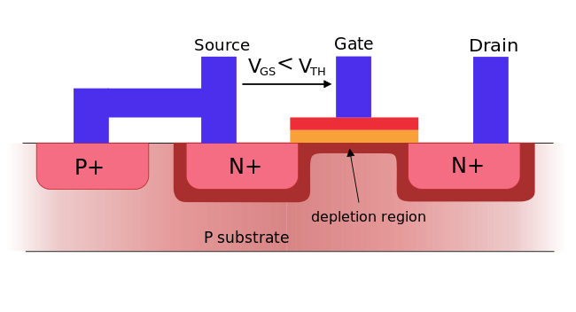
MOSFET Functioning Body / Biezl / CC BY SA
There’s more to it than just three terminals though. The actual structure of the MOSFET is critical to understanding why technologies such as HKMG and FinFET exist. In the case of an n-type MOSFET, the source and drain are wells of n-doped semiconductor, with a p-doped semiconductor substrate surrounding the two. In between the two is the gate, which is the metal-oxide-semiconductor portion that the MOSFET is named after.
The gate in a traditional MOSFET is rather simple. On top of the silicon substrate, a layer of silicon dioxide (SiO2) is generated, then a polysilicon or metal gate is placed on top of this SiO2 layer. This structure effectively makes the gate a capacitor, with SiO2 as the dielectric.
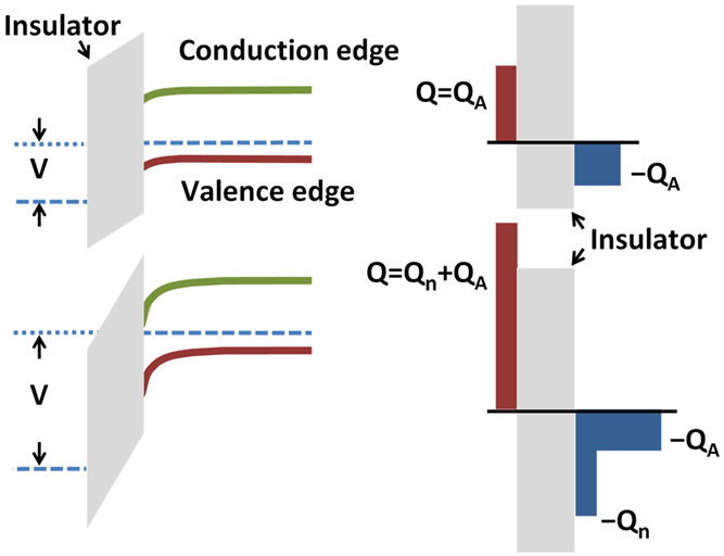
Semiconductor Band Bending / Bews Ohare / CC BY SA
Those that have taken some level of introductory physics will know that a capacitor generates an electric field if there is a voltage difference between the plates. While an electric field cannot go through a conductor due to the density of electrons/holes, the same is not true of a semiconductor. Once again, the Fermi level and band diagrams become important.
As a result of the electric field, the silicon of the body near the silicon dioxide has a higher chance of electrons with sufficient energy to become delocalized. This can be seen as band bending in the band diagram, where the conduction band stretches down past the Fermi level. Because the Fermi level is the total chemical potential of electrons, this means that it is much more likely for electrons to jump the band gap between the valence band and the conduction band. However, this comes at a cost.
As the density of electrons increases, the field effect becomes weaker and weaker. Thus, the band bending decreases until the effect is nonexistent. The point where this happens marks the end of the channel created. As a result of the concentration of free electrons, there is an inversion layer created. The reason why it’s an inversion layer is because in the case of this n-type MOSFET (or NMOS), the p-type body/substrate becomes an n-type substrate within the inversion layer.
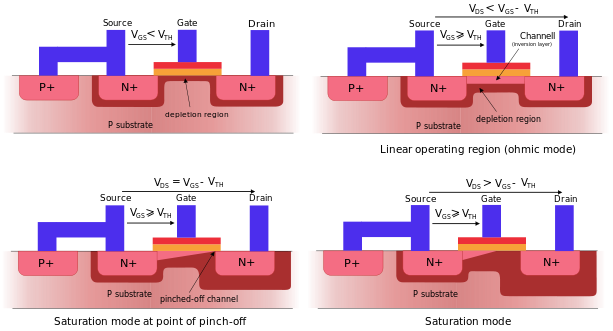
MOSFET Functioning / Olivier Deleage & Peter Scott / CC BY SA
As a result of the positive voltage on the gate, the inversion layer becomes a “channel” of sorts, which allows current to flow between source and drain. That’s how an NMOS works to control the flow of current from drain to source using a gate. Since the above photo also shows the regions that a transistor can operate in, it's important to understand that the linear operating mode is where the output current of the transistor is directly proportional with voltage. In the saturation mode, this is no longer true and diminishing returns are seen in current despite increasing voltage until the transistor reaches the maximum possible current. In a CMOS camera sensor this makes it difficult to accurately recover overexposed photos as this saturation mode causes the signal to be clipped, which is why underexposed photos are generally preferable to overexposed ones.
Now let’s look at a PMOS. The same is true, merely reversed. By applying a low voltage to the gate, an electric field pushes away electrons, forming a channel of holes that allows current to flow from source to drain. In the interest of avoiding confusion, we’ll avoid discussion depletion-mode MOSFETs for now although it may be worth revisiting at a later point. This is also because depletion-mode FETs effectively don’t exist in today’s processes.
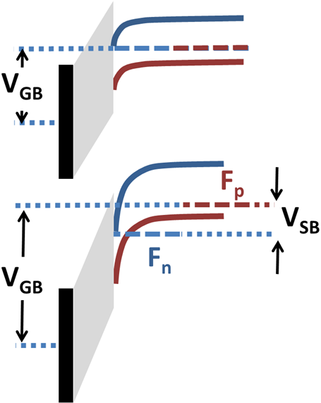
Inversion With Source-Body Bias / Brews Ohare / CC BY SA
Of course, I mentioned the body effect earlier on but never quite explained what it was. Now that we understand how the system works at a basic level, we can add a bit of complexity in the form of biasing on the body terminal. We talked about how applying a voltage to gate would cause the band structure to change. In the case of applying voltage to the body terminal, the same band-bending occurs and alters the threshold voltage on the gate needed to enter the linear region of transistor operation.
CMOS Logic
So now that we understand (maybe) how transistors work, the real question is how to implement logic using these gates. After all, it’s not immediately clear how controlling the flow of current translates into the sheer amount of possible instructions seen in code. While there are multiple methods to do this, this article will only cover the most popular method. This is known as complementary metal-oxide-semiconductor, or CMOS. The reason why this method of implementing logic is so popular is because of its power characteristics. While other methods have significant amounts of current draw regardless of state, CMOS only requires a significant amount of power while switching. We’ll go over why this is later.
Before I go over CMOS, I'll do a quick introduction to Boolean logic for those that are unfamiliar with the subject. In short, it's possible to take apart almost any statement and turn it into a series of logical operations. These operations are AND, OR, and NOT. While there are more operations than those three, every possible logical operation is possible through the combination of the three. This makes it possible to do math, store input and output, and all the other things we see in computing devices today. There's definitely much more to it, although that's best left for another day.
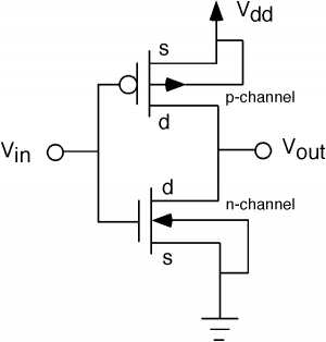
Now that we've done an extremely basic introduction of Boolean logic, CMOS is rather simple in its rules for implementing such logic. Through these rules, it’s possible to implement every possible logic gate, and we’ll go over the simplest example for CMOS, the NOT gate. CMOS is purely composed of p-type and n-type MOSFETs, with no need for resistors that would generate waste heat. There are only two rules that must be followed to be electrically considered a CMOS circuit:
1. All PMOS transistors must either have an input from the voltage source or another PMOS transistors.
2. All NMOS transistors must either have an input from ground or another NMOS transistor.
Using these two rules it is possible to build all the other gates. For example, the NOT gate simply requires one NMOS and one PMOS. The PMOS is connected to the voltage source and the NMOS to the ground. The gate for both is controlled by a single input, and the output current is also connected together. An example of this circuit diagram can be seen below. I've also included a link for a java applet that simulates this circuit here.
NOT Gate / OpenStax CNX
If the input voltage is high, the NMOS turns on and the PMOS is off. The result is that the output wire is pulled to the ground voltage, which is 0V. This would be measured as a low voltage. If the input voltage on the gate is low, then the PMOS will switch on. The result is that the output wire has a voltage close to Vdd, which is relatively high. If the truth table is written out, we can see that this matches exactly with the truth table for the NOT operation.
Of course, there are multiple other operators. While it might be worth going over for those interested in majoring in electrical or computer engineering, to keep things (relatively) simple we’ll avoid talking through how those circuits work.
Through billions of transistors arranged in the complementary fashion just described, entire CPUs are made. Of course, these aren’t individual pieces. These billions of transistors are on a single package no bigger than the size of a fingernail. For reference, A5X was one of the largest mobile SoCs ever shipped, and its die area is 163 square millimeters. Apple’s A6 SoC is only around 97 square millimeters, or smaller than a square with side length of a centimeter. The question now is how to squeeze all of these transistors into such a small area. To answer that, we must look at the manufacturing process.


77 Comments
View All Comments
Khenglish - Thursday, October 9, 2014 - link
Curving the wafer actually has major impacts on electronic operation. For example wafer bending is currently done by implanting Germanium into the wafer for PFETs. Because Ge is larger than Si, this causes the wafer to bend. This bend increases hole mobility making PFETs more conductive and faster, but slows down NFETs, thus manufacturers implant Ge only at PFET locations. This processes of bending the wafer by implanting Ge is strained silicon, and 1st started showing up around the 130nm era. It is done because for similarly sized transistors, NFETs are around 2.7x more conductive than PFETs without strained silicon.EMM81 - Monday, October 13, 2014 - link
There is definitely no curving or any wafer. Ge is used to strain the silicon crystal latice. Ge is in the same group on the periodic table and forms the same diamond cubic crystal structure. Grading a fraction of Ge (larger atoms longer bond lengths) into the Silicon latice the silicon bonds effectively get stretched (see image in article). This has a physical effect on the mobility of electrons and holes. Curving a wafer is a non-starter as NONE of the standard processing techniques would work...wafers have to be not only flat but ultra flat for litho optics, dry etch, wet etch spinners, ion implanters...hlovatt - Thursday, October 9, 2014 - link
Great article. More please!witeken - Thursday, October 9, 2014 - link
Awesome, thanks for the great article.However, 22nm doesn't have a single feature size of 22nm. It's just a name, and so are 28nm, 20nm, 16nm, 14nm,...
For example, the fins of 22nm are 8nm while the gate pitch is 90nm. (http://images.anandtech.com/doci/8367/14nmFeatureS...
Khenglish - Thursday, October 9, 2014 - link
When you hear 22nm, 32nm, 16nm, etc the number you are hearing is the smallest feature size that can be imprinted via lithography. This is not necessarily the smallest feature size than can be implemented on the process.EMM81 - Monday, October 13, 2014 - link
This is not true. Node size was loosely defined as the half pitch of either the poly-silicon gate or the tightest metal pitch. The node size designation however, has not followed the minimum half pitch for many technologies, from any of the fabs. Node size is now a purely marketing term. If a fab were to implement HKMG, strained silicon...these things would not necessarily have any effect on the dimensions of transistors but they would result in improvements to the chip performance. Density is only 1 component that plays into node designation these days and even then density of the transistors is being tightened by some fabs while leaving the density of the upper layers unchanged.Khenglish - Wednesday, October 15, 2014 - link
Again just because lithographic features can be made a certain size does not mean you make everything that size. Maybe there is just one minor feature that is really that size. I'm saying that process size is the minimum size that can cut by the ebeam into a lithography mask and transferred if the design calls for it. This is why when looking at a processor that the feature size is so hard to quantify. Just one feature at whatever they advertise can let them call it that number. Yes feature size doesn't need to have anything to do with density or performance and is mostly a marketing thing.Keisari - Thursday, October 9, 2014 - link
A very necessary article. Great initiative!martixy - Thursday, October 9, 2014 - link
There's probably something to be said about breezing through this(of my own free will moreover), while having such a hard time with the exact same material from the textbook.Go figure.
Murloc - Thursday, October 9, 2014 - link
It's meant to be intuitive and summarized in a limited amount of space. That's why it's easy to read. It has way less depth than a textbook.