An Introduction to Semiconductor Physics, Technology, and Industry
by Joshua Ho on October 9, 2014 3:00 PM EST- Posted in
- Semiconductors
- CMOS
- Physics
- Industry
- Technology
I must confess that until recently, I wasn’t well-versed in semiconductor physics or technology. While it’s rather easy to understand what a transistor does and some of the terminology thrown around, going deeper was tough. A great deal of the information on the internet is simply too cryptic to understand, even for those that want to learn. Seeing as how this site is all about the results of semiconductor physics and technology, this was the best place to share the knowledge that I've acquired.
Bandgap In Semiconductor / Pieter Kuiper
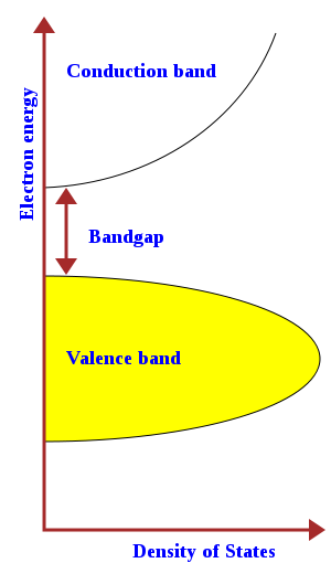
The simplest place to start is the materials. Silicon is incredibly important as a material in the industry because it’s a semiconductor. Of course, the name is self-explanatory, but there’s more to it. The key here is the band structure. Band structure refers to the “bands” of energy levels that form due to the sheer number of orbital states that can be occupied in molecules. Those that understand how electron orbitals work will point out that each energy level is discrete, but due to the sheer number of orbital configurations, a seemingly continuous distribution of energy can be seen. However, relatively large gaps still exist; known as a band gap, these are an energy state that an electron cannot occupy.

Band Filtering Diagram / Nanite
The question now is why this matters. The reason why it does matter is because of the Fermi level, or EF in the photo above. The Fermi level refers to the total chemical potential energy for a system of electrons at absolute zero. If the band lies above the Fermi level, electrons in the band can be delocalized from the atom, which means that it can carry current. This band is called a conduction band. If the band is below the Fermi level, this means that the electron is bound to an atom. This band would be a valence band.
Intrinsically, a semiconductor should have its Fermi level at the midpoint of the band gap. This is true of both insulators and intrinsic semiconductors, but a semiconductor’s band gap is extremely small. In fact, it’s small enough that electrons can jump the band gap as seen in the photo above because of thermal energy that will always exist in real world situations. While this property alone isn't particularly useful for digital logic, doping a semiconductor can have significant effects on the band structure. This means that the distribution of electrons in the valence band or conduction band will change.
This is where I have to introduce even more terminology. Depending on how the distribution is changed, a semiconductor is dubbed either a p-type or n-type semiconductor. If the band structure is such that free electrons are more easily generated, it becomes an n-type semiconductor. If the structure is such that electron “holes” are generated, it becomes a p-type semiconductor. In this case, electron holes refers to a place where an electron could exist, but doesn’t. Such a hole still conducts current. Look carefully at the p-type diagram once again. Because the valence band is so close to the Fermi level, electrons tend to stay in the valence band at lower orbitals. This is means that there are "holes" where an electron could be, which makes it a charge carrier. It's also worth noting that the diagram above isn't totally accurate, as doping normally introduces more bands instead of shifting their positions, but the concept is the same.
PN Junction Equilibrium / TheNoise / CC BY SA
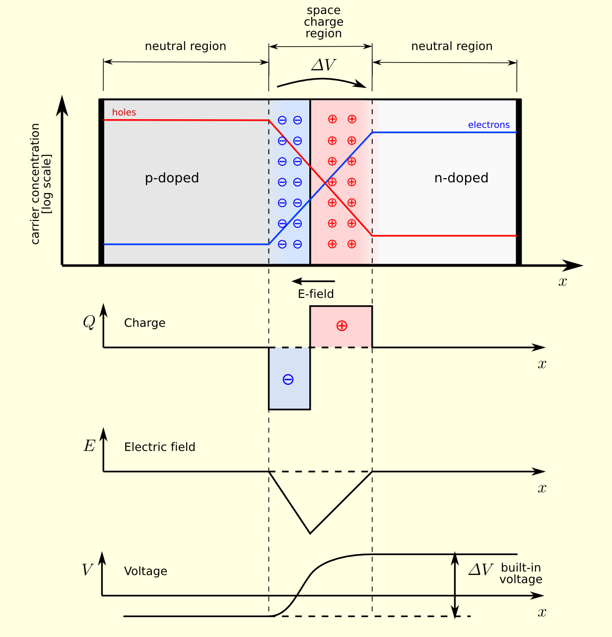
What really makes things interesting is when a p-type and n-type semiconductor are placed next to each other. Because p-type semiconductors tend to have electron holes and n-type semiconductors tend to have an excess of electrons, there will be a diffusion of holes and electrons to try and equalize charge at the junction. Because of this diffusion process, the area around the junction becomes charged positively at the n-doped region and negatively at the p-doped region. This happens because the n-doped region is losing electrons, making the area positive while the p-doped region is losing holes, therefore becoming negative. The result is that an electric field is generated which opposes this diffusion and eventually reaches equilibrium. The area where this process occurs is called the depletion layer, as these ionized areas are stripped of charge carriers and therefore unable to carry current with the band structure that already exists.

PN Band / Saumitra R Mehrotra & Gerhard Klimeck / CC BY
This p-n junction is incredibly important in solid state electronics. In fact, the system we just described can be used as a diode, which is a device that only allows current to flow in a single direction. If a battery is connected with the positive terminal at the p-type semiconductor and the negative on the n-type semiconductor, the holes in the p-type and the electrons in n-type are all pushed towards the junction, which causes the depletion zone to shrink. This means that the electric field repelling the current decreases, and current is allowed to flow across the junction.


77 Comments
View All Comments
danjw - Thursday, October 9, 2014 - link
I am wondering if we haven't already hit the limits of current technology. TSMC doesn't seem to be able to produce anything more powerful than a SOC for phones and tablets on their 20nm process. While Intel seems to think they will have 14nm desktop and notebook parts out in the second quarter of next year, I wonder if they really will. Right now all we have seen from them at 14nm is similar to what TSMC is able to do at 20nm.This really concerns me as far as technology stagnating until the next big thing comes along.
Homeles - Thursday, October 9, 2014 - link
There's no end in sight. About a year ago, perhaps a little earlier, the 7 or 5nm nodes were seen as the end of Moore's Law. Advancements have been made since then, though, and scaling past the 5nm node is very likely. 10nm's "recipe" is basically all finished at Intel at this point, with "all" that's left to do at this point being increasing the yields. EUV is making good progress, finally, and should be ready for insertion at Intel's 7nm node (if they skipped it for 10nm, which they likely did).14nm has been in production for quite some time now, with Broadwell first landing in tablets later this month. The chances that Broadwell won't make it to the desktop and notebook market around the middle of next year are essentially zero.
We're still also on schedule to have 450mm wafers introduced by the end of the decade, which would reduce costs by ~30%.
Even not looking at Intel, TSMC has millions of 20nm-based products on the market right now. 20nm is roughly twice as dense as its 28nm predecessor. It doesn't really make sense to be so skeptical of progress, given that the proof pudding has already been delivered.
danjw - Thursday, October 9, 2014 - link
All those 20nm products are not desktop or notebook CPUs or GPUs, which they lead AMD and Nvidia to believe they would be able to do. Intel is way behind its original estimates to get Broadwell out, and that just in table SOCs. Intel wanted badly to get Broadwell parts out for the new school year, then it was Christmas, now it is Q2 of 2015. Yes, I think there is plenty of reason to be skeptical.EMM81 - Monday, October 13, 2014 - link
Your facts are all incorrect...If you can produce an SOC you already have all of the capability to produce GPU's or CPU's since it has logic, SRAM and graphics components already. Broadwell parts are already in the hands of vendors NOW and are being sold this year and they are not SOC's they are low power full core chips. 14nm Broadwell chips are in no way equivalent to 20nm TSMC chips. A fab can use the additional capability of a new node in different ways. They can reduce density to make chips cheaper to make, increase performance, decrease power and all of these things will be done in different ratios depending on the product. You need to work on detailed reasoning and apples to apples comparisons.errorr - Thursday, October 9, 2014 - link
The problem is that the only real advancements are more expensive per transistor and I doubt they will change.The great thing about process shrinks is that it reduces the cost per transistor.
Also I doubt EUV will ever work. It has been almost ready and a couple years away for a decade. Tell me when you don't need MW levels of power to get usable light to a wafer and maybe I will consider it.
450mm wafers have also been just a couple years away for at least 15 years. I'll believe the 2020 hype when I actually see it.
The way to the next node is easy and everyone knows they can use triple patterning. Nobody wants that because of the expense is huge already and every single circuit would have to be redrawn due to limitations on the pokygons.
I don't know what's next but the only people expecting EUV to pan out are the people who have spent billions trying to make it work and failing.
ShieTar - Friday, October 10, 2014 - link
EUV is not "almost ready", it has been commercially available for 2 years now.http://www.zeiss.com/semiconductor-manufacturing-t...
Khenglish - Thursday, October 9, 2014 - link
The problem with smaller processes is not physically producing them. The problem is that they start getting slower than larger processes. This is due to 2 reasons.1. Narrower, more resistive interconnects.
2. Increase in channel doping levels due to not having enough dopant atoms to form a P-N junction as processes increase.
1. As process sizes shrink, so do interconnects. Resistance is dependent on cross sectional area and length of the wire. As you shrink a process, the cross sectional area drops at a squared rate, while length drops at a linear rate. The end result is that wires become linearly more resistive as the process shrinks. Keeping wire length down due to resistance is also a big reason why individual core transistor counts have not been going up significantly. The cores need to stay small to keep the wire length down. Repeaters to boost current drive ability on long wires has been around starting at around 90nm.
2. If you want a 10nm process, you probably have a gate length of 10nm. The volume of a 10nm cube is 10^-18 cm^-3. High doping levels are those above around 10^17 atoms per cm. If we take a high doping level of say 10^18 atoms per cm, then we have only one single dopant atom in the entire channel region of the transistor. This means that if you are one atom off, you lose a transistor, which is difficult not to do with over 1B transistors in a microprocessor. You can dope up to around 10^21 cm^-3, but then your electron and hole mobility are terrible. Mobility is directly proportional to how much current a transistor can push, so as mobility drops performance drops. See this link for what happens to mobility as dopant levels increase.
http://ecee.colorado.edu/~bart/book/mobility.gif
abufrejoval - Saturday, October 11, 2014 - link
From what I read the problem isn't as much phyiscal or technical feasability as economical viability: Moore's law was mostly about the ability to deliver more power at a lower price for the end consumer pushing the technology. Now the economical yields of process shrinks are diminishing to the point where further shrinks won't pay for themselves.DanNeely - Thursday, October 9, 2014 - link
If you're also interested in how simpler transistors are made; hack-a-day's hosted a video lecture from someone who was producing chips with a handful of transistors on them in her home lab a few years ago.http://hackaday.com/2010/03/10/jeri-makes-integrat...
anexanhume - Thursday, October 9, 2014 - link
Graphene isn't dead in the water. There are ways to create a bandgap, for example using bilayer graphene and introducing a gap via electric fields or doping.http://www-als.lbl.gov/index.php/contact/56-bilaye...
Then you can take advantage of its remarkable carrier mobility. Mass production remains a huge issue, and I also have concerns about its effect on living creatures and the environment. http://www.gizmag.com/graphene-bad-for-environment...