The Samsung Exynos 7420 Deep Dive - Inside A Modern 14nm SoC
by Andrei Frumusanu on June 29, 2015 6:00 AM EST
Over the past few years it’s been somewhat expected tradition for Samsung Electronics to employ a strategy of multi-sourcing the SoC for their mobile devices. Most notably it’s on the North American and specifically CDMA markets that we saw wide usage of Qualcomm SoCs. This diversification started with the Galaxy S2 as it was offered both in versions with Samsung System LSI's Exynos chipset as well as variants with Qualcomm’s Snapdragon offerings. On the last few generation of devices we’ve seen the average share of Exynos in Galaxy devices continually decline, as the shift to ARM's Cortex A15 based SoCs just didn’t work out as well in terms of power consumption and thus lost design wins to better balanced Krait-based SoCs from Qualcomm. In fact the last time we’ve seen a Galaxy device make use of an Exynos throughout all its global variants was the Galaxy Note 2 back in 2012.
With the Galaxy S6 again offering a world-wide release of exclusively Samsung designed SoCs, we see an immensely contrasted situation to what we had just over a year ago. The Exynos 7420 marks a true new generation of SoCs for Samsung. The chipset is described as the company’s “most advanced application processor to date”, and today we’re going to have a deep investigation into what a modern SoC looks like, and try to put the chip through its paces through power and performance measurements.
We’ve had a slight glimpse into what the Samsung’s Exynos 7420 might look like when we reviewed the Exynos 5433 in the Note 4 back in the beginning of the year. Attentive readers might remember that as far back as last September I called the Exynos 5433 more of a “brain-transplant” when it comes to SoC-design. This means that it looked like the chipset received an IP upgrade in form of new ARM's A5X series of CPU designs and a Mali T760 GPU, making this only an evolutionary design from other SoCs from last year such as the Exynos 5430 (A15/A7 + T628) and its predecessors. The Exynos 7420 might from a first glance look like nothing more than a process shrink and slight upgrade in the GPU configuration with LPDDR4 memory, but as we’ll soon see there are more details under the hood.
Investigating Samsung's 14nm Process
We’ve heard rumors about Samsung wanting to make a 14nm SoC as far back as 18 months ago. Samsung Semiconductor was historically a follower to TSMC in the leading-edge foundry manufacturing business, so the general consensus among analysts and most of the media was that this was just an unrealistic expectation given the fact that vendors had just started delivering out 20nm TSMC silicon late last year with Apple’s A8 and more recently Qualcomm's Snapdragon 810 and 808. Even though Samsung had presented working 14nm silicon as far back as early October (Which I highly suspect was the 7420) and has in several financial calls confirmed mass production late last year, it still came to many as a shock to actually see the Galaxy S6 be announced exclusively with the 14nm in-house SoC.
The 14nm process marks Samsung's transition from planar transistors to FinFET-based ones. Intel was well ahead of the rest of the industry to make this jump on their 22nm process which shipped in products in 2012, and we should be plenty familiar with the technology by now.
A great deal of discussion ensued over whether Samsung’s 14nm process really represented a “true” die shrink over its 20nm predecessor. We were ourselves surprised to see Chipworks announce that the piece came in at only 78mm² compared to the Exynos 5433’s 113mm². This 31% shrink was beyond what we expected, as we previously reported that Samsung’s 14nm process was to continue to use the 20nm’s BEOL (Back-End-Of-Line, a chip’s largest metal layer) and thus make for only a minor progression. Both the BEOL’s M1 metal pitch and the transistor’s contacted gate pitch equally determine the density and just how much a design is able scale in area on a given process. It was only after Samsung’s ISSCC February 2015 presentation on the Exynos 5433 (Credits to our colleagues at PC Watch) that it became clear as to what is going on:
While Samsung has in the past only referred to the 20nm node as a single process, the reality is that there seems to have been two planned variants of the node. The variant we’ve seen in The Exynos 5430 and 5433 was in fact called 20LPE. In contrast, the process of which 20nm borrows its BEOL from is another variant called 20LPM – and this node sees a very different M1 metal pitch. 20LPM looks to be a cancelled node as it was subsequently dropped in favor of the 14nm processes. We can summarize the differences between Samsung’s recent manufacturing processes in the following table.
| Samsung Semiconductor Manufacturing Processes | ||||||
| 28LPP | 20LPE | 20LPM (Cancelled) |
14LPE | |||
| Nominal VDD | 1.0V | 0.9V | 0.87V | 0.8V | ||
| Logic CPP | 113.4nm | 90nm | 86nm | 78nm | ||
| M1 Metal | 90nm | 80nm | 64nm | 64nm | ||
| M1 * CPP Density | 10206 | 7200 | 5504 | 4992 | ||
Taking the product of the M1 pitch times the contacted gate/poly pitch (CPP) gives an overall representative measurement of process density, and here we incidentally see the same 31% shrink that we saw that happened between the Exynos 5433 and Exynos 7420.
| Samsung Exynos Block & Die Sizes (mm²) |
||||||
| Exynos 5420 (28nm LPP) |
Exynos 5430 (20nm LPE) |
Exynos 5433 (20nm LPE) |
Exynos 7420 (14nm LPE) |
|||
| Big Core | 2.74 | 1.67 | 2.05 | 1.20 | ||
| Big Cluster | 16.49 | 14.50 | 15.10 | 8.88 | ||
| Little Core | 0.58 | 0.40 | 0.70 | 0.48 | ||
| Little Cluster | 3.80 | 3.30 | 4.58 | 2.71 | ||
| GPU Cluster | 30.05 | ~25.00 | ~25.00 | 17.70 | ||
| SoC Total | 136.96 | 110.18 | 113.42 | 78.23 | ||
When we are looking at the block sizes between the 5433 and 7420, we see this theoretical shrink only apply for the individual A53 cores. Both the individual A57 cores and total cluster saw a much large shrink of 59%. The total GPU size also went down by 30% - but keeping in mind that the 7420 has two additional shader cores over the 5433’s MP6 configuration this is also represents a big difference. A single T760 core on the 7420 comes in at 1.75mm², so if we would subtract 3.5mm² from the total area of 17.70mm², we’d end up with a total of 14.2mm for a hypothetical 14nm MP6 GPU – which then again would represent a massive 56% shrink over the Exynos 5433’s GPU if we assume things remained equal on shared common blocks.
This very large ~56%+ shrink of some of the main IP blocks points out that Samsung was not only able to take advantage of the theoretical shrink due to the process, but also further tweaked the physical implementation by either employing more efficient cell libraries or by optimizing the layout for density. When considering the above findings, we can now see how Samsung managed to achieve what is a rather lightweight SoC when looking at the historical die sizes of previous chipsets while still managing to stuff in two additional GPU cores and a LPDDR4 memory controller among other changes.
Evaluation of a process node outside of high-tech laboratories is always a tricky thing as we need to rely on measurable external characteristics such as voltage and power. For some vendors it’s hard to even read out a SoC’s voltages - for example the furthest I was able get with HiSilicon SoCs was to read the PMIC’s register values, but without knowing a buck converter’s indirect mapping to actual voltage it still remains a mystery as to under what operating level the silicon is running at. Luckily this isn’t the case for Samsung SoCs, and in our review of the Galaxy S6 we’ve already been able to present a preview/summary of how voltages were affected when compared to the Exynos 5433 20nm process. To recap some example cases of how voltages have dropped, here’s again a table of operating voltages among a few common frequencies and binning groups of the two chipsets:
| Exynos 5433 vs Exynos 7420 Supply Voltages | ||||||
| Exynos 5433 | Exynos 7420 | Difference | ||||
| A57 1.9GHz (ASV9) | 1200.00mV | 975.00mV | -225.00mV | |||
| A57 1.9GHz (ASV15) | 1125.00mV | 912.50mV | -212.50mV | |||
| A57 800MHz (ASV9) | 900.00mV | 687.50mV | -224.50mV | |||
| A57 800MHz (ASV15) | 900.00mV | 625.00mV | -275.00mV | |||
| A53 1.3GHz (ASV9) | 1112.50mV | 950.00mV | -162.50mV | |||
| A53 1.3GHz (ASV15) | 1062.50mV | 900.00mV | -162.50mV | |||
| A53 400MHz (ASV9) | 787.50mV | 656.25mV | -131.25mV | |||
| A53 400MHz (ASV15) | 750.00mV | 606.25mV | -143.75mV | |||
| GPU 700MHz (ASV9) | 1050.00mV | 800.00mV | -250.00mV | |||
| GPU 700MHz (ASV15) | 1012.50mV | 750.00mV | -262.50mV | |||
| GPU 266MHz (ASV9) | 800.00mV | 668.75mV | -131.25mV | |||
| GPU 266MHz (ASV15) | 762.50mV | 606.25mV | -156.25mV | |||
In the S6 review we briefly described how ASV (Adaptive Scaling Voltage) is Samsung’s denomination for the silicon binning process. Process variations during manufacturing can lead silicon to have different electrical characteristics, leading to cases where a product would no longer be able to function properly under its target specifications. On the desktop space we're familiar with the common practice of disabling parts of the silicon to be able to recycle a “bad piece” into a lower priced SKU. Currently I’m not aware of any semiconductor vendor following this method in the mobile space as there simply isn’t the same opportunity to recycle chips into lower performing SKUs. What does very commonly happen though is that vendors try to increase voltages to compensate for such process variations, overcoming problematic manufacturing issues in this way. Chipsets are tested at the factory for their characteristics and each chip is then permanently marked with the information by burning it to on-chip fuses.
For the Exynos chipsets these bins are called ASV groups. The groups with the higher voltages represent bins with “slow-” or “cold” silicon, meaning process variations cause transistors to not to be fully able to reach the design frequency without having to raise VDD from the nominal targets. One advantage of cold chips is that their static leakage is reduced over other bins. On the other spectrum we have “fast” or “hot” silicon with lower threshold voltages that are able to hit the desired clock-rate at a lower VDD. In contrast to cold silicon, hot silicon has much more static leakage due to the lower Vt. Power consumption in today’s large SoCs is mostly determined by the dynamic leakage (gate to drain, drain-induced barrier lowering, etc) of a chip as it overshadows static leakage currents which can be mitigated by power-gating mechanisms. FinFET also comes into play as it helps to dramatically reduce static leakage compared to planar technologies. It is thus certainly almost always more advantageous to have a “hot / fast” bin which is able to reach lower operating voltages.

As seen in the graphic, the range between a worst-case and best-case for the Exynos 7420 can be as high as 150mV which represents up to 32% more dynamic power on the highest frequency of the A57 cores. Luckily, one should not have to worry too much about the bin in one’s device as shipped units follow a Poisson distribution pattern where the vast majority of chipsets fall at or around the lambda of ASV10-ASV11. I’ve yet to see a report of somebody receive a device of <ASV6, which doesn’t mean they don’t exist, but they may be very rare. The device which we’ve tested power on in this article came with a chipset graded ASV10 (Highlighted in green in the graph) on the CPU clusters and memory controller and ASV11 on the GPU, which by the way also points out to the fact that the main SoC blocks are individually characterized and don’t necessarily fall in the same grading/bin category.
Until now I’ve been careful to refer to voltages as “target voltages”, and although it’s true that buck converters (High efficiency step-down voltage regulators) on the PMIC may not be fully accurate when providing that voltage, what I’m referring to is another voltage control mechanism outside of the usual software DVFS (Dynamic Voltage and Frequency Scaling) control. For this year, Samsung introduced a new closed-loop DVS (Dynamic Voltage Scaling) system in the Exynos 7420. A closed-loop system is a control system that operates on a feedback loop which continuously monitors inputs through sensors, in this case hardware performance monitors (HPMs). In the case of a DVS system, what we are talking about is a microcontroller which chooses a certain voltage to tell the regulator to apply, and HPMs on the SoC’s various voltage planes. In the Exynos 7420, we see this being arbitrated by an on-chip Cortex M3 microcontroller. Samsung names this the APM- although I’m not sure what it stands for, but strongly suspect it’s either Advanced or Adaptive Power Manager.
The Cortex M3 which we’ll refer to as the APM from now on, communicates with the main system only via small mailbox messages. Mailboxes are one method of inter-processor communication between differing architectures, with each processor can only write messages to their own mailbox (RAM space), but can read all other mailboxes. The overlying software DVFS mechanisms running on the Linux kernel sends target voltages to the APM whenever there’s a frequency change. At first the kernel and main CPU also programs the PMIC regulator directly via an i2c interface, but after the frequency change control is then handed over to the APM until the next frequency change. The APM in turn measures HPMs, one each located on both CPU clusters as well as on the GPU and the memory controllers. When the APM sees the voltage threshold fall, either due to temperature or other influences changing the silicon’s characteristics, it takes advantage of it to further lower the voltages below the values of the stock voltage tables determined by the binning process.
The advantage of the APM over software based solutions by the main CPUs is that it able to have finer granularity and real-time response; it changes voltages at a 1ms interval, compared to the current 20-80ms sampling period the main DVFS mechanism runs at. Voltage steps depend on the PMIC used on the device, for the Galaxy S6’s this means 6250µV granularity on the main buck converters. I’ve noticed Samsung experimented with different margins on how far the APM was allowed to undervolt, and it currently sits at 25mV for the CPU cores and 12.5mV for the GPU and memory interface.
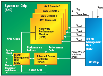
Texas Instruments' PowerWise technology represents a similar closed-loop voltage mechanism (Credit: TI)
What is unusual about this closed-loop voltage regulation system is not the system itself, but the fact that Samsung uses it in conjunction with traditional binning. Texas Instruments was one of the first players in the mobile space to apply CL systems for voltage regulation and was employed in various OMAP SoCs. PowerWise AVS was meant to be used as a power management mechanism – but more importantly it is supposed to cut production cost as it removes the characterization and binning process from the production chain. Qualcomm in the Snapdragon S810 and Nvidia in the Tegra K1 are two other vendors who’ve recently switched over to closed-loop systems, and similarly to TI, they’ve dropped traditional fixed binned voltage tables and rely solely on HPMs to dictate the operating voltages.
Samsung’s 14nm process together with the aforementioned improved voltage regulation systems end up providing a quite massive voltage reduction compared to the Exynos 5433 and previous SoCs. I was curious to see just how low I could go, and was able to achieve down to around 587mV on the A53 cores without taking into account the APM margins. The memory interface is the lowest supplied voltage plane on the 7420, as it operates at a stock value of 575mV up until the 416MHz state before it needs to go higher. The same plane on the Exynos 5433 didn’t go under 750mV.
Earlier in the year I made the comment that while Samsung rolled out 20nm SoCs relatively early compared to other vendors other than Apple, it didn’t really represent a clear competitive advantage as TSMC’s 28HPM process set the bar very high for 2014. Fast-forward only a few months and we see a very different competitive landscape as Samsung beat TSMC to FinFET technology not only by 6-9 months, but actually delivered much more than was initially revealed in the official announcements. It will be interesting how the industry shifts towards the 14nm process as Samsung and process partner GlobalFoundries continue to ramp up production capacity and TSMC also starts to mass produce its own 16nm FinFET node.


114 Comments
View All Comments
JoshHo - Wednesday, July 8, 2015 - link
We have responded to his concerns. These benchmarks are independently run and not provided by either ARM or any division of Samsung. We have re-run the benchmarks and verified that the benchmark is placed on the right cluster. However, we will look into recompiling our version to see if we can get more representative values.mmrezaie - Monday, June 29, 2015 - link
Thanks, a very nice article.kspirit - Monday, June 29, 2015 - link
I like how power efficient this thing is. Thanks for the review!Badelhas - Monday, June 29, 2015 - link
Great artcile, as usual.The big question is to know if the performance is noticeable under Samsung´s Touchwiz, which tends to lag as hell.
theduckofdeath - Monday, June 29, 2015 - link
What?! You didn't manage to get it in there first? We're We all sleeping over at the troll office? :Dnathanddrews - Monday, June 29, 2015 - link
Nice one, English Bob!GC2:CS - Monday, June 29, 2015 - link
The power efficiency improvements from FinFet are really huge which makes me that excited about the next gen Apple SoC built on TSMC's 16nm FF process !Couldn't be an Apple SoC's deep dive looking into power consumption made then ?
That would be super interesting.
Andrei Frumusanu - Monday, June 29, 2015 - link
An Apple SoC deep dive as detailed as what was done here just isn't possible due to the closed nature of iOS. For example the CPU power curves just aren't feasible as there's no power management control for CPU frequency. We could do maximum power consumption and the GFXBench tests, but that's about as far as it gets.jjj - Monday, June 29, 2015 - link
The new power saving mode downclocks the SoC so you could have an extra data point, depending on what are the other actions in this mode. And who knows maybe it can be edited?CiccioB - Monday, June 29, 2015 - link
In theory TMSC 16+nm PP should not allow for a shrink of the die, as it is the same 20nm PP with FinFet support. Power consumption should go down, but density will not.