Comparing Snapdragon 810 v2 and v2.1: More Memory Bandwidth, Higher Clocks
by Joshua Ho on June 18, 2015 9:00 AM EST
Around a few weeks before the launch of the Xiaomi Mi Note Pro, I was digging through kernel source to understand Snapdragon 810 and some other Qualcomm SoCs. We had kept track of MSM8994v1 and MSM8994v2, which were relatively well understood in terms of what they represented. V1 was an engineering sample variant, which was discussed as early as September in 2014. This variant set both the A57 and A53 clusters to a ~1 GHz maximum. V2 was the first mass production revision, which was present in both the LG G Flex 2, and HTC One M9. However, shortly before the launch of the Mi Note Pro, we noted references to v2.1 in various kernel source trees.
Immediately diving into the issue, what I found was that there wasn’t much of note about v2.1 other than a change to the chip ID and other identifying information, so any formal information on the changes between these revisions is scarce. Meanwhile phones that definitely didn’t have this variant of the SoC still had references to it in kernel source, which only made it all the harder to even identify v2.1 devices in the first place. Ultimately the only way to truly verify whether a device has a certain revision of an SoC is to either see whether the file is included in the compilation process or to verify the revision by checking the device itself.
Our big break came with the release of the Xiaomi Mi Note Pro, which was among the first (if not the first) devices to incorporate a v2.1 SoC. After getting our hands on a sample of the Mi Note Pro, we were finally able to start piecing together everything in order to really understand what was going on with this new variant.
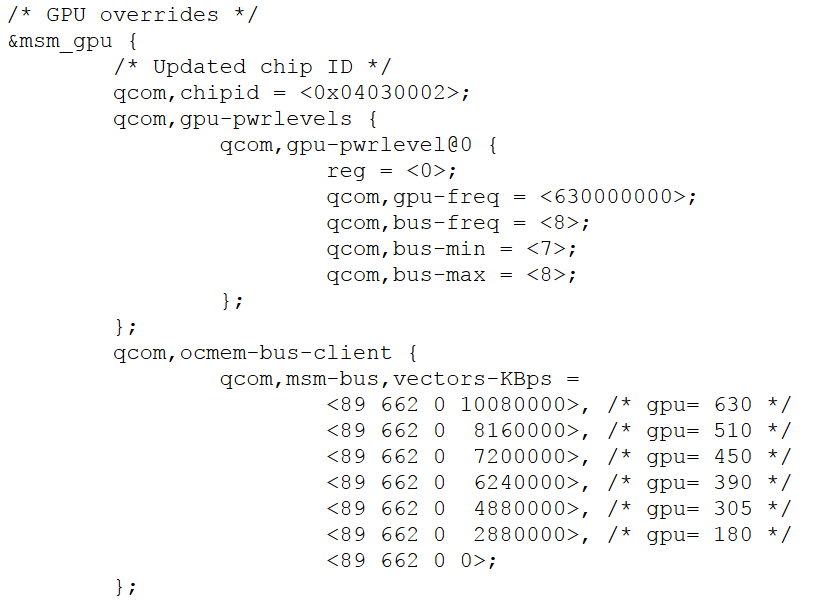
The first and most obvious change in v2.1 is a mild increase in GPU clocks from 600 to 630 MHz. This represents around a 5% increase in performance, which helps to close the gap with the 772-700 MHz Mali T760MP8 graphics processor used in the Exynos 7420 of the Samsung Galaxy S6. This is fairly obvious to anyone that runs a graphics benchmark on this new variant, although this is a best-case improvement as inefficiencies elsewhere can erode the difference.
The other differences are far more subtle. The first is that there’s noticeably less throttling on the A57 cluster compared to Snapdragon 810 v2. However even with that change - and unlike the Snapdragon 808 and competing SoCs - both variants of the Snapdragon 810 still see the unfortunate characteristic of ultimately forcing all threads off of the A57 cluster to stay within TDP limits in high load conditions, such as when running Basemark OS II’s battery test.
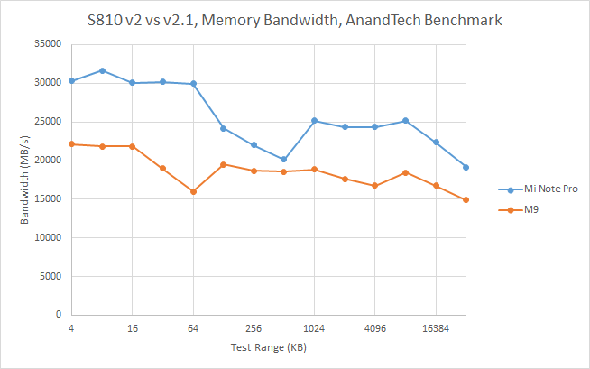
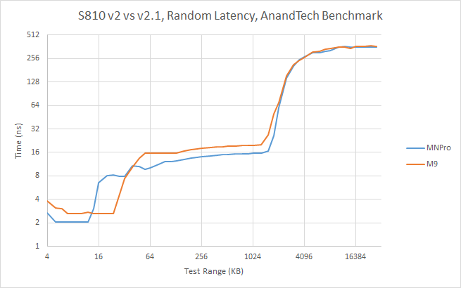
The second difference requires testing peak CPU bandwidth and latency between L1, L2, and main memory, which required digging into our in-house benchmark tools. In the interest of seeing 810's maximum memory bandwidth, we put together a memory multithreaded memory benchmark that runs on multiple CPU cores, and combines read and write bandwidth to try and get as close as possible to maximum bandwidth available. The figures that we present here will represent a scenario where two threads, one reading and one writing will load the memory system simultaneously. This is done to try to saturate the main memory controller and to circumvent some of the quirks of ARM's bus architecture, which has dedicated read and write ports, leading to only half the total possible bandwidth in each direction.
We’ve also tested against multiple other applications such as Rahul Garg’s RgBandwidth and RamBench to verify these observations. We also checked with instrumented runs that the CPU, memory controller, and CCI interconnect were all running at appropriate frequencies so these results should be largely unaffected by the governor due to the 100% duty cycle of the load during the test.
The graphs above are interesting, but they don’t really illustrate the relative difference between v2 and v2.1. To better show this, the graphs below represent the percent difference between the HTC One M9 and Xiaomi Mi Note Pro in this test, where positive values are an advantage in favor of Mi Note Pro, while negative values represent an advantage in favor of the One M9.
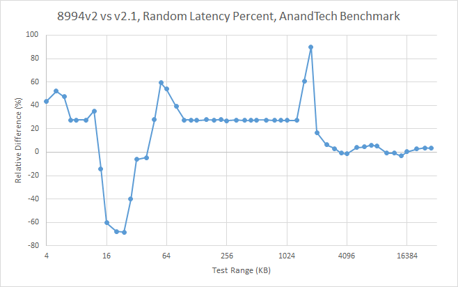
From the calculations, memory latency improves on an average of 15%, but this is mostly concentrated in the L1/L2 cache portion of the test, while the differences in DRAM are relatively small. If we change the scaling to show less of main memory, we can see that most of the variance is present in that portion of the test. Given that we’re looking at time on the order of nanoseconds, I wouldn’t think too hard about these differences either. The only interesting thing to note in the latency test is that the “memory mountain” model is still valid, where we can expect about an order of magnitude increase in latency for each level of cache that we miss, where L1 appears to take about 5 cycles at 2 GHz, then around 15 cycles for L2, then around 600-700 cycles for main memory. (To put that into comparison for PC CPUs, L3 cache usually hits up to 70 cycles and up to 150 cycles for Intel's CrystalWell eDRAM before the jump out to main memory.)
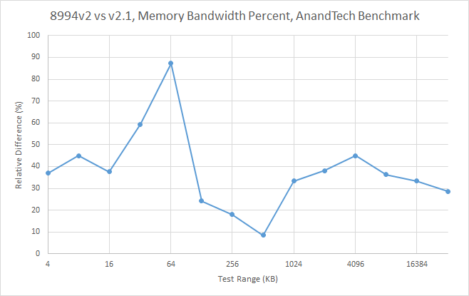
The memory bandwidth values are really much more interesting though, as there’s a consistent improvement in bandwidth across the board. There is some interesting behavior around L1 cache, but this is likely due to the previously mentioned ramp time for frequency scaling. If we just look beyond L2, into the main memory, the result is that there’s around a 33% increase in bandwidth, and a 38% average increase if we look at the entire sweep through memory.
Overall, for a 0.1 revision, Snapdragon 810 v2.1 is a pretty significant change where memory is concerned. We also see some improvements in terms of thermal management, but we yet have to fully characterize just how much this improvement is and if it's enough to be able to compete with Samsung's 14nm silicon in the Galaxy S6.
Meanwhile there were rumors floating around of a new revision due to show up in the summer, and it appears that this is the rumored revision. This leads me to question whether it made sense to release devices with the v2 revision, especially if future revisions would have resolved some notable issues and dramatically improved SoC performance. I also question whether OEMs would silently introduce these SoCs into later production runs of products that first shipped with v2, which is yet another can of worms.
Putting these questions aside, this new revision brings much-needed improvements to the Snapdragon 810, and should go a long way as a stop-gap until Snapdragon 820 begins shipping. We'll see how the change from v2 to v2.1 affects performance on a higher level in our Xiaomi Mi Note Pro review coming shortly.


84 Comments
View All Comments
PhytochromeFr - Friday, June 19, 2015 - link
lol. 810's A57 core consumes over 4 watt per core. it can't sustain full clock for 2 core less than 10 sec. http://tieba.baidu.com/p/3819195171?pn=0&testbug00 - Friday, June 19, 2015 - link
that testing is deffo flawed.PhytochromeFr - Friday, June 19, 2015 - link
yes. it has little flaw. he measured whole system power load. so we need to get rid of power usage of other parts. but, after subtract other part's power consumption(subtract power usage at A53 1 core load), it still over 4 watt.testbug00 - Friday, June 19, 2015 - link
That's a funny joke. Seriously, that test is incorrect. That, or it is deliberately screwed up.I suspect (S)he managed to have 2 A57 cores running, no matter what the results say in the end. Qualcomm builds their platform around an unmodified A57 core. You'll find an unmodified core draws under 2.5 watts at 2.1Ghz.
chizow - Thursday, June 18, 2015 - link
Why so many revisions of the 810? Didn't Qualcomm publicly state there were no yield or perf issues on the 810 months ago? And now we see all this constant tweaking, OEMs choosing to downgrade to the 805, their own chips or other SoCs for their flagships.1 bad chip from Qualcomm won't fully erode confidence in them, but 810 has been awful for them.
testbug00 - Thursday, June 18, 2015 - link
As far as CPU and GPU performance goes there is no issue if cooled in a chassis capable of dissipating 10W+In smaller form factors you hit a thermal and power wall well before that. The thermal wall hitting earlier than it should due to the broken memory controller.
So, technically, Qualcomm's wording can be taken as correct as far as performance goes. 'performance' is such a vague word. No clue about yields. It's around the size of Apple's A9 iirc, so, shouldn't be any any problems there.
Refuge - Thursday, June 18, 2015 - link
If I add an * to any statement I make, I can make it true also.It doesn't change the fact that this chip is too hot for the form factor that it is supposed to target.
testbug00 - Thursday, June 18, 2015 - link
Notice how Qualcomm's reference design device was a tablet...? And it ran fine at full clocks.Refuge - Monday, June 22, 2015 - link
Ok, so this SoC was meant for tablets, and all the other manufacturers just threw their hands up and said "Whatever, we do what we want!"?Either that or I mis-understood your post, because this was definitely targeted at every flagship smartphone.
retrospooty - Friday, June 19, 2015 - link
"1 bad chip from Qualcomm won't fully erode confidence in them, but 810 has been awful for them"Yup. With any chip really, you have to wait until its tested on actual shipping product, not engineering samples. Dont believe pre-release hype, don't believe PR, don't believe fanboys. When its independently tested by a few trusted sites then and only then can you believe it.