NVIDIA Discloses Next-Generation Tegra SoC; Parker Inbound?
by Joshua Ho on January 5, 2016 4:31 AM EST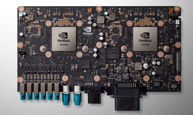
While NVIDIA has been rather quiet about the SoC portion of the DRIVE PX 2, it’s unmistakable that a new iteration of the Tegra SoC is present.
The GPUs and SoCs of the DRIVE PX 2 are fabricated on TSMC’s 16nm FinFET processes, which is something that we haven’t seen yet from NVIDIA. The other obvious difference is the CPU configuration. While Tegra X1 had four Cortex A57s and four Cortex A53s, this new SoC (Tegra P1?) has four Cortex A57s and two Denver CPUs. As of now it isn’t clear whether this is the same iteration of the Denver architecture that we saw in the Tegra K1. However, regardless of what architecture it is we’re still looking at a CPU architecture that is at least partially an ARM in-order core with a wide, out of order VLIW core that relies on dynamic code optimization to translate ARM instructions into the VLIW core ISA.
Based on the description of the SoC, while NVIDIA is not formally announcing this new SoC or giving it a name at this time, the feature set lines up fairly well with the original plans for the SoC known as Parker. Before it was bumped to make room for Tegra X1, it had been revealed that Parker would be NVIDIA's first 16nm FinFET SoC, and would contain Denver CPU cores, just like this new SoC.
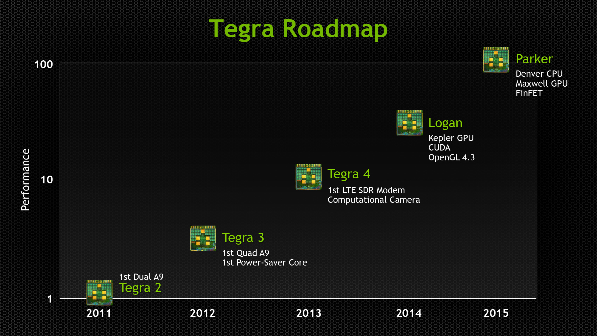
NVIDIA's Original 2013 Tegra Roadmap, The Last Sighting of Parker
Of course Parker was also said to include a Maxwell GPU, whereas NVIDIA has confirmed that this new Tegra is Pascal based. Though with Parker's apparent delay, an upgrade to Pascal makes some sense here. Otherwise we have limited information on the GPU at present besides its Pascal heritage; NVIDIA is not disclosing anything about the number of CUDA cores or other features.
| NVIDIA Tegra Specification Comparison | ||||
| X1 | 2016 "Parker" | |||
| CPU Cores | 4x ARM Cortex A57 + 4x ARM Cortex A53 |
2x NVIDIA Denver + 4x ARM Cortex A57 |
||
| CUDA Cores | 256 | ? | ||
| Memory Clock | 1600MHz (LPDDR4) | ? | ||
| Memory Bus Width | 64-bit | ? | ||
| FP16 Peak | 1024 GFLOPS | ? | ||
| FP32 Peak | 512 GFLOPS | ? | ||
| GPU Architecture | Maxwell | Pascal | ||
| Manufacturing Process | TSMC 20nm SoC | TSMC 16nm FinFET | ||
But for now the bigger story is the new Tegra's CPU configuration. Needless to say, this is at least somewhat of an oddball architecture. As Denver is a custom CPU core, we’re looking at a custom interconnect by NVIDIA to make the Cortex A57 and Denver cores work together. The question then is why would NVIDIA want to pair up Denver CPU cores with also relatively high performng Cortex A57 cores?
At least part of the answer is going to rely on whether NVIDIA’s software stack either uses the two clusters in a cluster migration scheme or some kind of HMP scheme. Comments made by NVIDIA during their press conference indicate that they believe the Denver cores on the new Tegra will offer better single-threaded performance than the A57s. Without knowing more about the version of Denver in the new Tegra, this is somewhat surprising as it’s pretty much public that Denver has had issues when dealing with code that doesn’t resemble a non-branching loop, and more troublesome yet code generation for Denver can take up a pretty significant amount of time. As we saw with the Denver TK1, Cortex A57s can actually be faster clock for clock if the code is particularly unfavorable to Denver.
Consequently, if NVIDIA is using a traditional cluster migration or HMP scheme where Denver is treated as a consistently faster core in all scenarios, I would be at least slightly concerned if NVIDIA decided to ship this configuration with the same iteration of Denver as in the Tegra K1. Though equally likely, NVIDIA has had over a year to refine Denver and may be rolling out an updated (and presumably faster) version for the new Tegra. Otherwise it also wouldn’t surprise me if the vast majority of CPU work for PX 2 is run on the A57 cluster while the Denver cluster is treated as a co-processor of sorts, in which only specific cases can even access the Denver CPUs.


23 Comments
View All Comments
darkich - Tuesday, January 5, 2016 - link
Alright AT..where the heck is your iPad Pro review?!?!?Oldair - Tuesday, January 5, 2016 - link
Since PX2 is 8tflops, and its a dual soc, would the Single tegra SOC be 4tflops, or at least around there, because if so, then that would make it way ahead of today's current gen consoles.psychobriggsy - Tuesday, January 5, 2016 - link
Nope, because there's also two Pascal GPUs (3 TFLOPS or thereabouts each) on board too.extide - Tuesday, January 5, 2016 - link
That 8GLOPS includes the 2 discreet pascal GPU's as well.Yojimbo - Tuesday, January 5, 2016 - link
One thing I think it would be safe to assume is that Denver has been worked on in the 18+ months since Denver TK1, and that the core used in Drive PX 2 is not the same iteration as that used in TK1. It seems useless to speculate whether it has the same performance characteristics of the previous version or not.But even if it did, other things to consider are that Drive PX 2 is a compute-oriented setup, and Pascal supports unified memory. The Drive PX 2 system is designed for the particular workload of machine learning for self-driving cars. The type of stuff going to be run on these machines is well known, so they should be able to much more finely tune what gets executed by what, I am guessing?
Finally, unlike last year with the Drive PX where NVIDIA said Drive PX was powered by two Tegra X1's, NVIDIA didn't announce an SOC name being used with the Drive PX 2. That seems like an indication that this particular SOC configuration isn't planned to be marketed outside of Drive PX 2 or similar in-house systems.
eddman - Tuesday, January 5, 2016 - link
It's probably as you wrote. It is quite possible that their phone/tablet variant of Parker will be different from the one in PX 2.vladx - Wednesday, January 6, 2016 - link
Nvidia dropped out off the phone market entirely.lucam - Wednesday, January 6, 2016 - link
and it also seems it's getting away from tablets too focusing entirely on automotive.psychobriggsy - Tuesday, January 5, 2016 - link
I think we're looking at 384 CUDA cores at around 30% higher clocks, to achieve around 1 TFLOPS FP32.And the Pascal GPUs are 3 TFLOPS (likely verified by 24 DLTOps figure).
3 + 3 + 1 + 1 = 8 TFLOPS - the number quoted for the device overall.
extide - Tuesday, January 5, 2016 - link
Sounds about right to me.