Original Link: https://www.anandtech.com/show/16640/arm-announces-neoverse-v1-n2-platforms-cpus-cmn700-mesh
Arm Announces Neoverse V1, N2 Platforms & CPUs, CMN-700 Mesh: More Performance, More Cores, More Flexibility
by Andrei Frumusanu on April 27, 2021 9:00 AM EST- Posted in
- CPUs
- Arm
- Servers
- Infrastructure
- Neoverse N1
- Neoverse V1
- Neoverse N2
- CMN-700
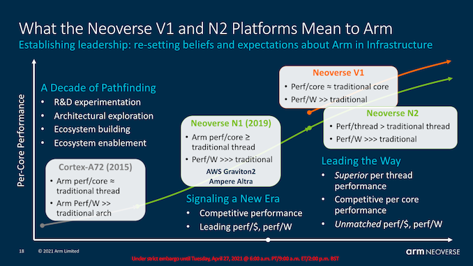
2020 has been an extremely successful year for Arm’s infrastructure and enterprise endeavours, as it was the year where we’ve seen fruition of the company’s “Neoverse” line of CPU microarchitectures hit the market in the form of Amazon’s new Graviton2 design as well as Ampere’s Altra server processor. Arm had first introduced the Neoverse N1 back in early 2019 and if you weren’t convinced of the Arm server promise with the Graviton2, the more powerful and super-sized Altra certainly should have turned some heads.
Inarguably the first generation of Arm servers that are truly competitive at the top end of performance, Arm is now finally achieving a goal the company has had in their sights for several years now, gaining real market share against the x86 incumbents.
Fast-forward to 2021, the Neoverse N1 design today employed in designs such as the Ampere Altra is still competitive, or beating the newest generation AMD or Intel designs – a situation that which a few years ago seemed farfetched. We recommend catching up on these important review pieces over the last 2 years to get an accurate picture of today’s market:
- Arm Announces Neoverse N1 & E1 Platforms & CPUs: Enabling A Huge Jump In Infrastructure Performance
- Amazon's Arm-based Graviton2 Against AMD and Intel: Comparing Cloud Compute
- The Ampere Altra Review: 2x 80 Cores Arm Server Performance Monster
- AMD 3rd Gen EPYC Milan Review: A Peak vs Per Core Performance Balance
- Intel 3rd Gen Xeon Scalable (Ice Lake SP) Review: Generationally Big, Competitively Small
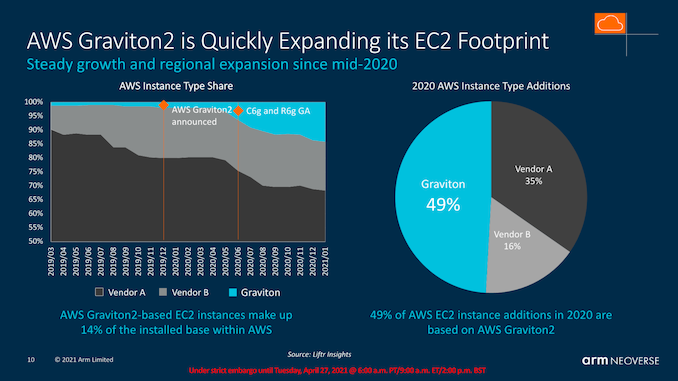
(Note: Y axis left chart starts at 50%)
Arm is very open that their main priority with the Neoverse line of products is gaining cloud footprint deployment market share, and as an example of the new-found success is an estimate into Amazon’s own AWS instance additions throughout 2020, where the new Arm-based Graviton2 is said to be the dominant hardware deployment, picking up the majority of share that’s being lost by Intel.
Looking towards 2022 and Beyond
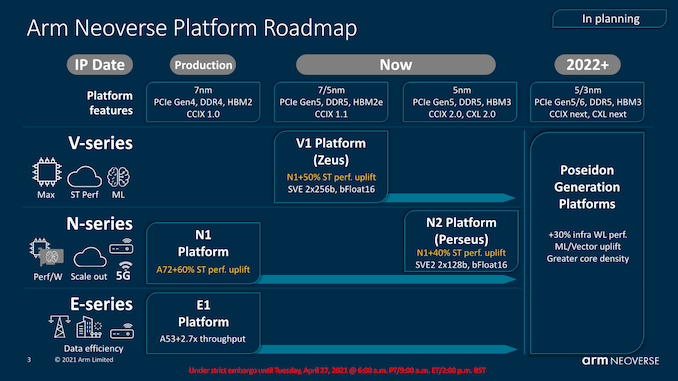
Today, we’re pivoting towards the future and the new Neoverse V1 and Neoverse N2 generation of products. Arm had already tested the new products last September, teasing a few characteristics of the new designs, but falling short of disclosing more concrete details about the new microarchitectures. Following last month’s announcement of the Armv9 architecture, we’re now finally ready to dive into the two new CPU microarchitectures as well as the new CMN-700 mesh network.
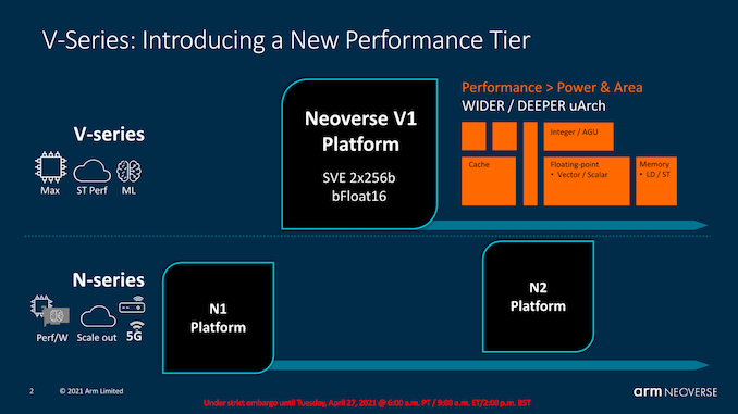
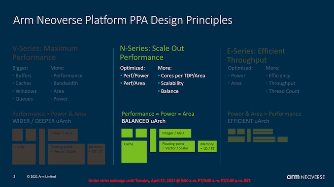
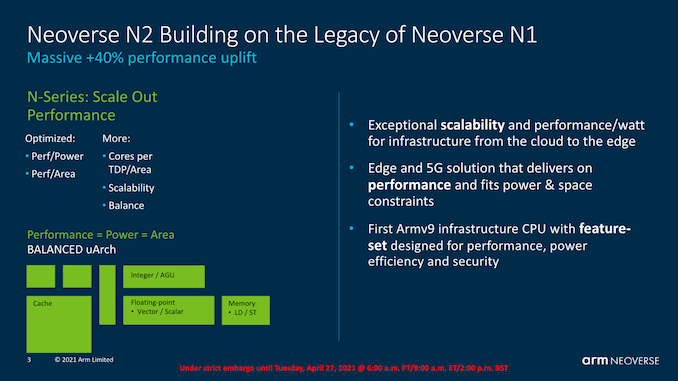
As presented back in September, this generation of Neoverse CPU microarchitectures differ themselves in that we’re talking about two quite different products, aimed at different goals and market segments. The Neoverse V1 represents a new line-up for Arm, with a CPU microarchitecture that is aiming itself for more HPC-like workloads and designs oriented towards such markets, while the Neoverse N2 is more of a straight-up successor to the Neoverse N1 and infrastructure and cloud deployments in the same way that the N1 sees itself today in products such as the Graviton or Altra processors.
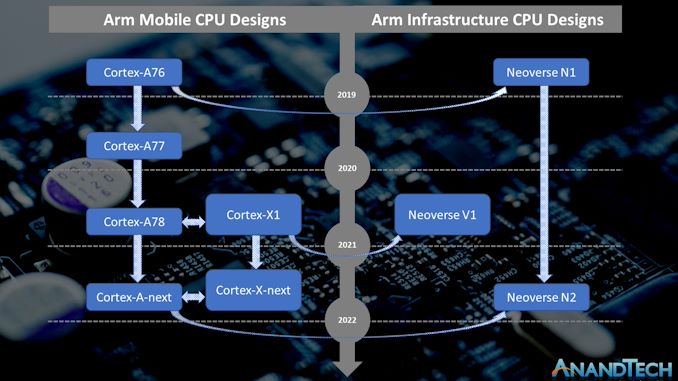
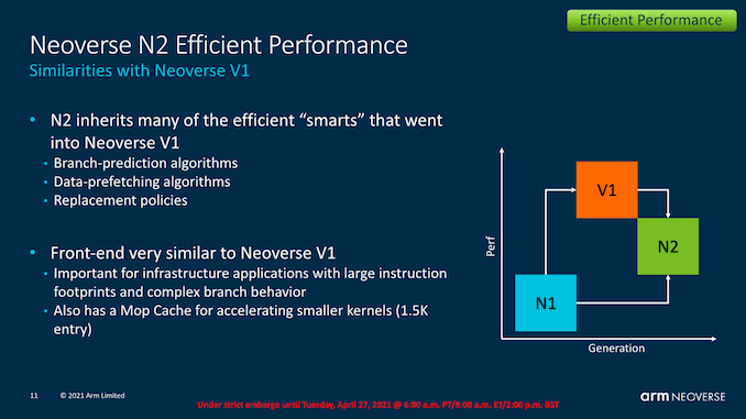
For readers who are familiar with Arm’s mobile CPU microarchitectures, there’s definitely very large similarities between the designs – even though Arm’s marketing seems to be oddly reluctant to make such kind of comparisons, which is why I made the above chart which more clearly tries to depict the similarities between design generations.
The original Neoverse N1 as seen in the Graviton2 and Altra Q processors had been a derivative, or better said, a sibling microarchitecture, to the Cortex-A76, which had been employed in the 2019 generation of Cortex-A76 mobile SoCs such as the Snapdragon 855. Naturally, the Neoverse designs had server-oriented features and changes that aren’t present in the mobile counterparts.
Similarly to how the N1 was related to the A76, the new generation V1 and N2 microarchitectures are related to newer designs in the Cortex-portfolio. The V1 is related to the Cortex-X1 which we’ve seen in this year’s new mobile SoCs such as the Snapdragon 888 or Exynos 2100. The Neoverse N2 on the other hand is related to an upcoming new Cortex-A microarchitecture which we expect to hear more about in the following few months. Throughout the piece today we’ll make a few more references to this generational disconnect between the V1 and N2, and it’s important to remember that the N2 is a newer design, albeit aimed at different performance and efficiency points.
This decoupling of design goals between the V1 and N2 for Arm comes through the company’s attempt to target more specific markets where the end products might have different priorities, much like how in the mobile space the new Cortex-X series prioritises per-core performance while the Cortex-A series continues to focus on the best PPA. Similarly, the V1 focuses on maximised performance at lower efficiency, with features such as wider SIMD units (2x256b SVE), while the N2 continues the scale-out philosophy of having the best power-efficiency while still moving forward performance through generational IPC improvements.
In today’s piece, we’ll be diving into the new microarchitectural changes of the V1, N2, as well as Arm’s newest generation mesh interconnect IP, the CMN-700, which is expected to serve as the foundation of the next-generation Arm infrastructure processors.
Table of contents:
- A Successful 2020 for Arm - Looking Towards 2022
- The Neoverse V1 Microarchitecture: X1 with SVE?
- The Neoverse V1 Microarchitecture: Platform Enhancements
- The Neoverse N2 Microarchitecture: First Armv9 For Enterprise
- The SVE Factor - More Than Just Vector Size
- PPA & ISO Performance Projections
- The CMN-700 Mesh Network - Bigger, More Flexible
- Eventual Design Performance Projections
- First Thoughts & End Remarks
The Neoverse V1 Microarchitecture: X1 with SVE?
Starting off with the new Neoverse V1, the design is both of a familiar origin, but also has a few distinct features that we see for the first time ever in an Arm CPU. As noted in the introduction, the V1 was designed at the same time as the Cortex-X1 by the same team at Arm’s Austin design centre, with large similarities between the two microarchitectures when it comes to the block structures.
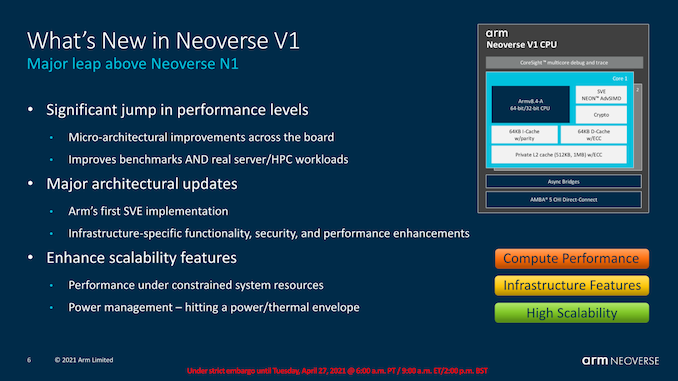
What’s notable about the V1, in comparison to the X1 and of course the predecessor N1, is the fact that this is now an SVE capable processor, with two native 256b SIMD pipelines, and also introducing server-only features such as coherent L1I caches, bFloat16 execution capabilities, and a slew of distinct characteristics we’ll cover in just a bit.
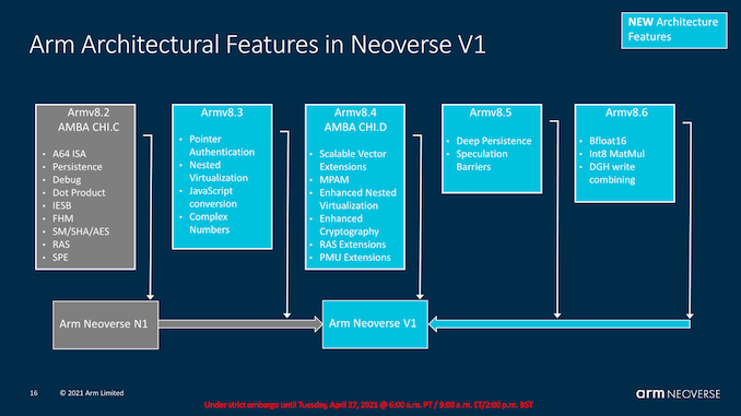
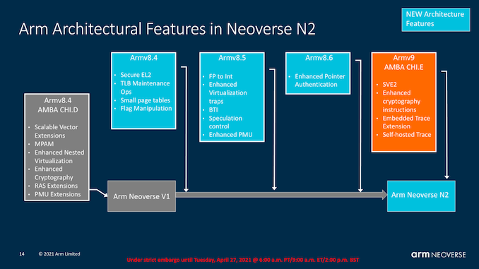
The architectural features of the Neoverse V1 are probably the most complicated in terms of describing – essentially, it’s a v8.4 baseline architecture which also pulls v8.5 and v8.6 features in for the HPC oriented workloads the design is aimed for. Given that we talked about Armv9 only a month ago, this may seem a bit odd, but again we have to remember that the V1 has been designed some time ago and that customers have had the IP for quite a while now, taping in or having already taped out V1 processors.
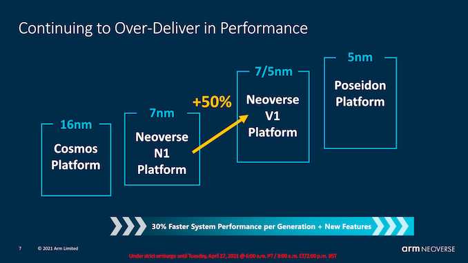
The big promise of the V1 is its extremely large performance jump over the N1, coming in at an IPC increase of +50%. This sounds large, and it is, but it’s also not all that surprising given that the microarchitecture essentially is 2 microarchitecture design generations newer than the N1, even through from a infrastructure product standpoint it’s only one generation newer.
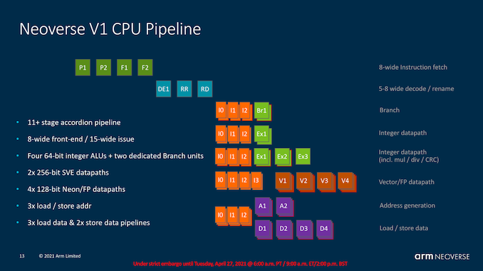
From a high-level pipeline standpoint and microarchitecture view, the Neoverse V1 is very similar to the X1. It’s still an extremely short pipeline design that has a minimum of 11 stages, with Arm putting a lot of focus on this aspect of their microarchitectures to reduce branch misprediction penalties as much as possible. This aspect of the microarchitecture has remained relatively static over the last few iterations of the Austin family of designs starting with the A76, so Arm notes that the frequency capabilities of the V1 is essentially unchanged when compared to the N1, with performance boosts coming solely from increased IPC.
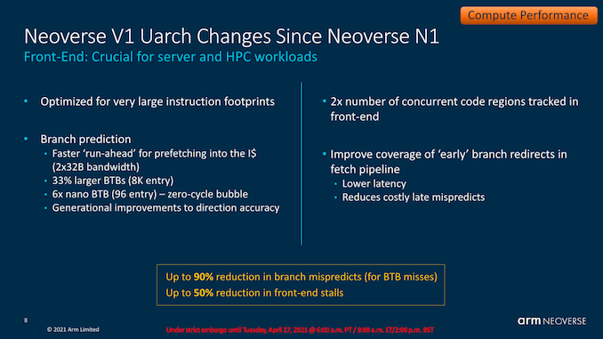
The V1 sees a lot of the front-end improvements we’ve seen with the Cortex-A77 and Cortex-X1 generations, which saw larger front-end branch improvements such as a doubled up bandwidth for the decoupled fetch unit, much larger L2 BTB to up to 8K entries, and a rearranging and resizing of the lower level BTBs, with the L0 (nanoBTB) growing to 96 entries, and the L1 BTB (microBTB) no longer being present when compared to the Neoverse N1.
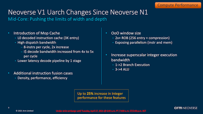
The V1 one when compared to the N1 also adds in new structures that hadn’t been present in the design, such as the introduction of a macro-Op cache of up to 3K decoded instructions. The dispatch bandwidth from the Mop cache is 8-wide, while the actual instruction decoder this generation is 5-wide, much the same as on the X1.
The out-of-order windows size is essentially doubled when compared to the Neoverse N1, with the ROB growing to 256 entries. This is actually a tad larger than what Arm was willing to disclose for the Cortex-X1 where the company had only talked about a “OoO window size of 224”, so in this regard this seems to be a differentiation to what we’ve seen in the X1.
On the back-end integer execution pipelines, the design also pulls in the many changes we’ve seen with the A77 generations, which amongst others include a doubling of the branch execution ports, and a new complex ALU capable of simple instructions such as additions as well as more complex operations such as multiplications and divisions.
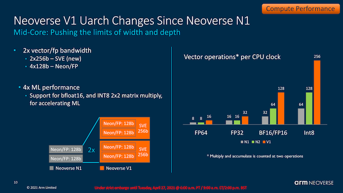
Obviously enough, the new SIMD pipelines are very different on the V1 given that this is Arm’s first ever SVE capable microarchitecture. The design has two pipelines with seemingly two dedicated schedulers, with native capability for 256b wide SVE vectors. The design is fully backwards compatible for 128b NEON/FP operations in which the pipelines then essentially act as 4x128b units, meaning it has the same execution width as the X1 in that regard.
Compared to the N1, the new design also supports new bFloat16 and Int8 data formats which greatly increase the AI and ML inferencing performance capabilities of the core.
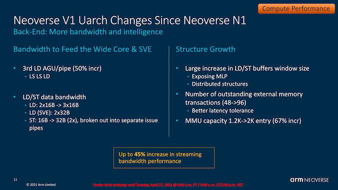
On the memory subsystem side, we also see the increased unit count found on the Cortex-X1, including 2 load/store units and one load unit, meaning the core is capable of up to 3 loads per cycle and 2 stores per cycle maximum. SVE vector bandwidth is 2x32B per cycle for loads, and 32B per cycle for stores.
The core naturally includes the data parallelism improvements seen on the X1 in order to increase MLP (Memory-level parallelism) capabilities.
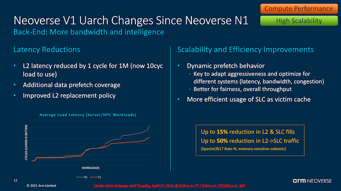
The L2 cache has also adopted a similar design to that of the X1, which is now 1 cycle faster at the same 1MB size, and has double the number of banks in order for increased access parallelism.
Arm here discloses a quite large reduction in the system level latency for the V1. Besides structural improvements, new generation prefetchers are a big part of this, such as the introduction of a new type of temporal prefetcher which is able to latch onto arbitrary access patterns over time and recognise subsequent iterations of the same pattern, and pull the data in.
Arm discloses that the core has new dynamic prefetching behaviour that plays a major role in reducing L2 to interconnect traffic, which is a critical metric in large core count systems where every byte of bandwidth needs to be of actual use and cannot be wasted for wrongly speculated prefetching.
The Neoverse V1 Microarchitecture: Platform Enhancements
Aside from the core-side microarchitectural aspects of the V1, the new design also features some new system-facing novelties that promise to help vendors integrate the CPU IP better in larger scale implementations.
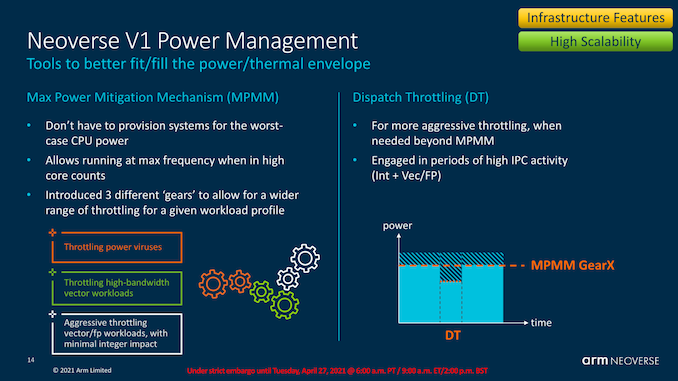
MPAM, or Max Power Mitigation Mechanism is a new fine-grained (to around 100 clock cycles) power management mechanism that promises to help smooth out the power behaviour of the core, and allow vendors’ implementations of the chip’s power delivery mechanisms to be so to say, be built to lesser requirements.
As we’ve seen in our review of the Ampere Altra, instead of fluctuating frequency at maximum TDP like how most x86 CPUs behave right now, the chip rather prefers to stay most of the time at maximum frequency, with the actual power consumption many times landing in at quite below the TDP (maximum allowed power consumption). A mechanism such as MPAM would allow, if possible, for the system’s average frequency to be higher by throttling the power limited cores to a finer degree. The mechanism to which this can be achieved can also include microarchitectural features such as dispatch throttling where the core slows down the dispatched instructions, smoothing out high power requirements in workloads having high execution periods, particularly important now with the new wider 2x256b SVE pipelines for example.
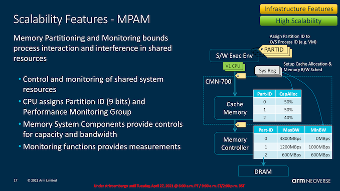
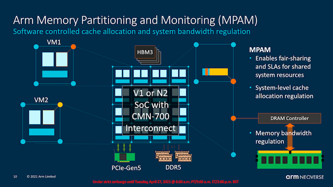
MPAM is a different mechanism helping interactions in larger system implementations. The Memory partitioning and monitoring feature is supposed to help with quality of service and reducing side-effects of noisy neighbours in deployments where multiple workloads, such as multiple VMs or processes, operate on the same system. This naturally requires software-hardware cooperation and implementation, but should be something that is particularly helpful in cloud environments.
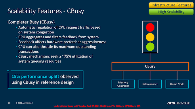
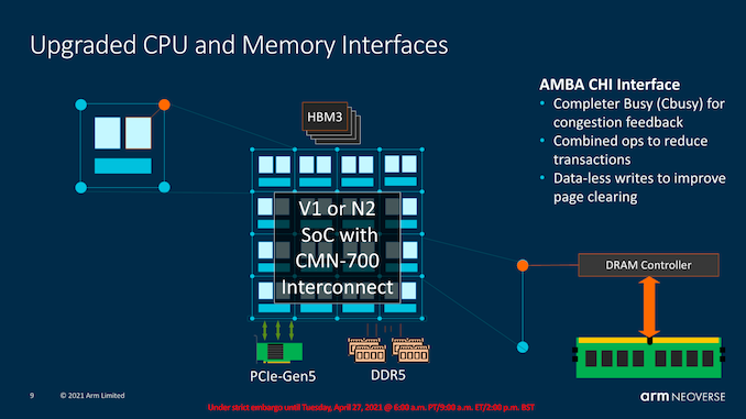
CBusy or Completer Busy is also a new system-side mechanism where the CPU cores interact with the mesh interconnect on a feedback-based basis, where the CPUs can vary their memory prefetcher aggressiveness depending on the overall mesh and system memory load. This ties in with the previously mentioned dynamic prefetcher behaviour where one can have the best of both worlds – better prefetching for more performance per core when the bandwidth is available, and very conservative prefetching when the system is under high load and there’s no room for wasted speculative bandwidth and data transfers.
The Neoverse N2 µArch: First Armv9 For Enterprise
Moving from the performance oriented Neoverse V1 to the more balanced Neoverse N2 core, we’re seeing a different approach to performance, more akin to the Cortex-A78’s PPA focus versus the X1’s performance focus.
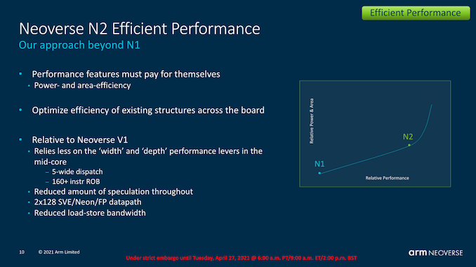
Arm makes note of the “balance” keyword here – the microarchitecture only adopts features and design changes if those changes actually contribute to an increase of the PPA (Performance, Power, Area) equation of the IP. In contrast, the V1 would opt for performance increasing features even if that meant a disproportionate increase in power and area, reducing the total PPA of the design.
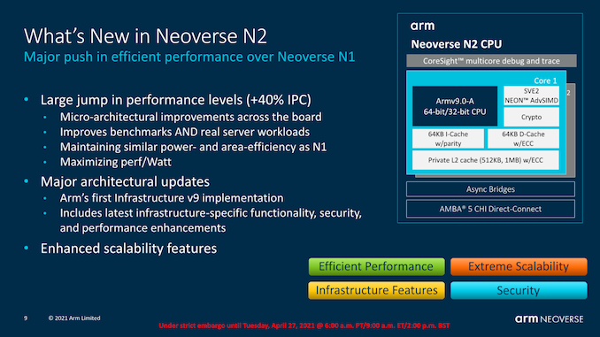
Architecturally, the N2 is a newer core than the V1 and takes a higher architectural baseline as the foundation of its capabilities. It’s Arm’s first disclosed Armv9 capable core, including important new features such as SVE2. It’s to be noted that although Arm talked a lot about Armv9 CCA (Confidential Compute Architecture) last month, the Neoverse N2 core does not feature this capability, which is an extension we’re told to expect in future microarchitecture designs.
Arm’s microarchitectural disclosures on the N2 were rather limited compared to the details we’ve seen on the V1. This being a sibling core to the yet undisclosed next generation Cortex-A78 successor, we’ll have to wait a few more months to see exactly what differentiates this newer iteration compared to the Cortex-A78, besides the notable Armv9 features and new SVE2 pipelines.
Arm at least confirms that it’s a narrower microarchitecture in the sense that there’s only a 5-wide dispatch (compared to 8-wide in the V1), and the design features 2x128b native SVE2 and NEON pipelines.
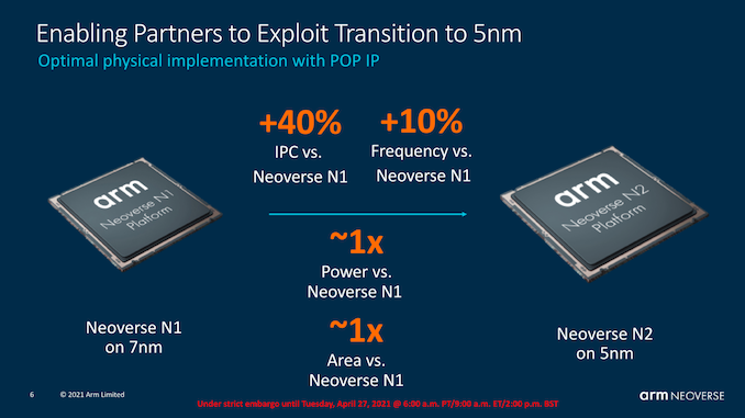
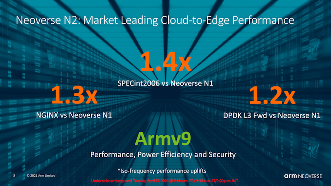
The company states that the new design should still achieve an impressive +40% increase in IPC compared to the Neoverse N1, which is actually substantial given the fact that we’re promised only a linear increase in power and area.
In terms of “smarts”, or better said, microarchitectural innovations, the N2 is a super-set of the V1, just with a more conservative approach to block and structure sizes.
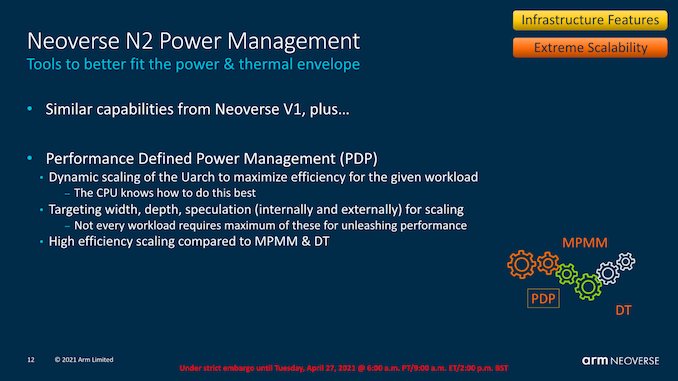
System side features, on top of MPMM and DT, PDP, or Performance Defined Power Management is a feature newer to the N2 that promises to vary the CPU’s microarchitectural features depending on workloads, in order to reduce power consumption without impacting performance. I imagine here that we’re talking about smarter workload dependent clock-gating of microarchitectural features, for example narrowing of the execution resources in low-IPC workloads.
The SVE Factor - More Than Just Vector Size
We’ve talked a lot about SVE (Scalable Vector Extensions) over the past few years, and the new Arm ISA feature has been most known as being employed for the first time in Fujitsu’s A64FX processor core, which now powers the world’s most performance supercomputer.
Traditionally, employing CPU microarchitectures with wider SIMD vector capabilities always came with the caveat that you needed to use a new instruction set to make use of these wider vectors. For example, in the x86 world, we’ve seen the move from 128b (SSE-SSE4.2 & AVX) to 256b (AVX & AVX2) to 512b (AVX512) vectors always be coupled with a need for software to be redesigned and recompiled to make use of newer wider execution capabilities.
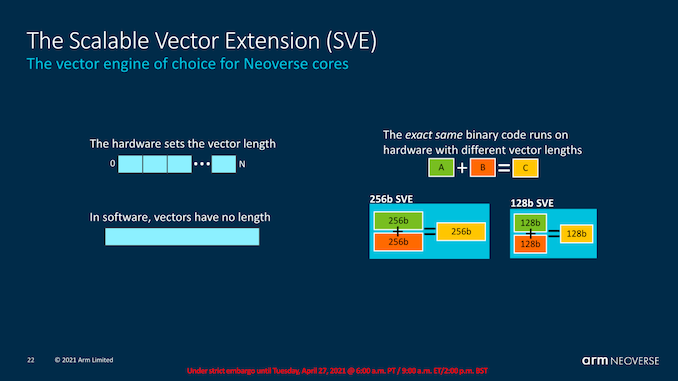
SVE on the other hand is hardware vector execution unit width agnostic, meaning that from a software perspective, the programmer doesn’t actually know the length of the vector that the software will end up running at. On the hardware side, CPU designers can implement execution units in 128b increments from 128b to 2048b in width. As noted earlier, the Neoverse N2 uses this smaller implementation of 128b units, while the Neoverse V1 uses 256b implementations.
Generally speaking, the actual execution width of the vector isn’t as important as the total execution width of a microarchitecture, 2x256b isn’t necessarily faster than 4x128b, however it does play a larger role on the software side of things where the same binary and code path can now be deployed to very different target products, which is also very important for Arm and their mobile processor designs.
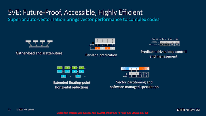
More important than the actual scalable nature of the vectors in SVE, is the new addition of helper instructions and features such as gather-loads, scatter-stores, per-lane predication, predicate-driven loop control (conditional execution depending on SIMD data), and many other features.
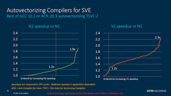
Where these things particularly come into play is for allowing compilers to generate better auto-vectorised code, meaning the compiler would now be capable of emitting SIMD instructions on SVE where previously it wasn’t possible with NEON – regardless of the vector length changes.
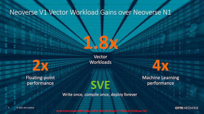
Arm here discloses that the performance advantages on auto-vectorizable code can be quite significant. In a 2x128b comparison between the N1 and the N2, we can see around 40th-percentile gains of at least 20% of performance, with some code reaching even much higher gains of up to +90%.
The V1 versus N1 increase being higher comes natural from the fact that the core has double the vector execution capabilities over the N1.
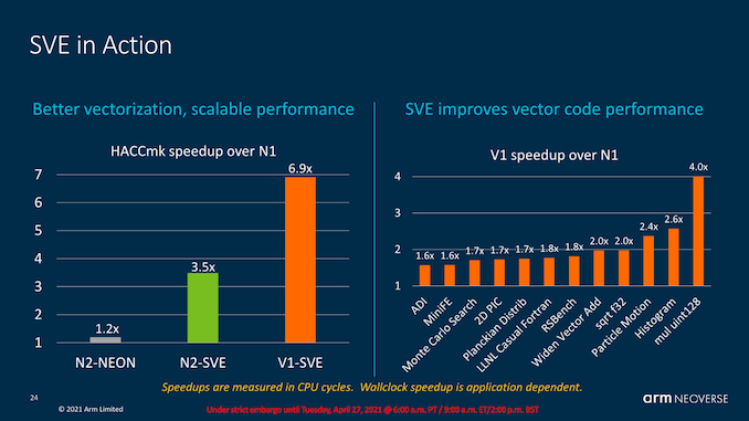
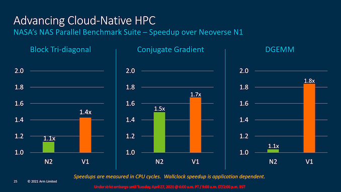
In general, both the N2, but particularly the V1, promise quite large increase in HPC workloads with vector heavy compute characteristics. It’ll definitely be interesting to see how these future designs play out and how SVE auto-vectorisation plays out in more general purpose workloads.
PPA & ISO Performance Projections
We’ve noted about the microarchitectural changes in the new V1 and N2 processors, as well as their IPC improvements, but it’s important to actually put things into context of the actual performance and power requirements to reach those figures. Arm presented an ISO-process node figures of what we can expect out of the designs:
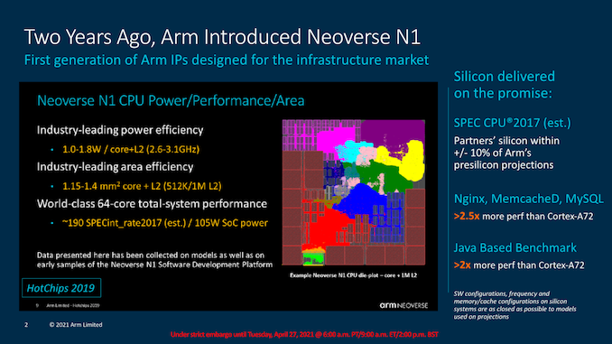
Starting off, we’re presented with a refresher of where exactly the Neoverse N1 was projected to end up. Back in 2019, the company had noted that an N1 core with 1MB L2 would take roughly 1.4mm² of area, and use up to 1.8W at 3.1GHz (TSMC 7nm node projection).
We’ve generally seen more conservative implementations (Graviton2) and more aggressive implementations (Altra Q) of the N1, but Arm states that their original presilicon projections ended up within 10% of the actual silicon performance figures of the respective products.
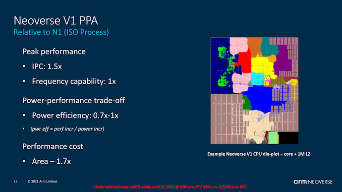
Compared to an N1, the V1 is meant to achieve 50% higher IPC, or 1.5x its predecessor while maintaining the same frequency capabilities.
What’s important to note on the slide here is that Arm is stating that power efficiency ranges from 0.7x to 1x that of the N1. Reversing the calculation for power usage increases, we actually end up with a 1.5x to 2.14x increase, which is actually quite significant. Arm also notes that the core is 1.7x larger than the N1, which is also a significant figure.
SiPearl’s Rhea chip was the first publicly known Neoverse V1 design and it features 72 cores on a N6 process node. The V1 core’s vastly increased power consumption means that it’s going to be incredibly hard to achieve similar clock frequencies while remaining in the similar 250W TDP range such as that of a current-gen top-end 80-core Altra chip, so either the core will have higher TDPs, or running at lower frequencies.
Arm also projects further non-ISO process performance figures which we’ll cover just a bit later, but there the company showcases a reference design of the V1 with 96 cores on 5nm at 2.7GHz. This means that whilst the microarchitecture seemingly would have the same frequency capabilities, the much higher power consumption of the core puts a practical limit onto the maximum frequency of any such larger core count designs.
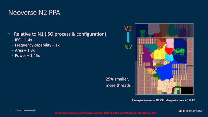
The Neoverse N2 seems a more appropriate design. Only losing out 10% IPC versus the V1, its power consumption is targeted to be only 1.45x higher than that of an N1, meaning efficiency lands in at an almost equal 96%. The area usage here is also only 1.3x that of an N1.
So generally speaking, the N2 seems to be a linear increase in performance over the N1 – both in performance and power. While this is not a regression in efficiency (well a small one at least), it does actually mean that in terms of frequency and end-performance targets, new N2 designs require larger generational process node improvements for actual vendors to be able to actually achieve the larger IPC and performance improvements that the new microarchitectures are promising.
I take note again of situations and workloads on the Ampere Altra where we’ve seen that there’s lots of workloads where the chip operates at below the TDP because the CPUs are underutilised. If an N2 design would be able to raise performance in such workloads, and more heavily throttle itself in higher demanding high utilisation workloads, it would still mean a net positive performance benefit even regardless of process node progresses. It’s a balance and situation that will be interesting to see how it plays out in eventual Neoverse N2 products.
In terms of absolute IPC improvements, Arm also disclosed a more varied set of workloads and what to expect out of the V1 and N2.
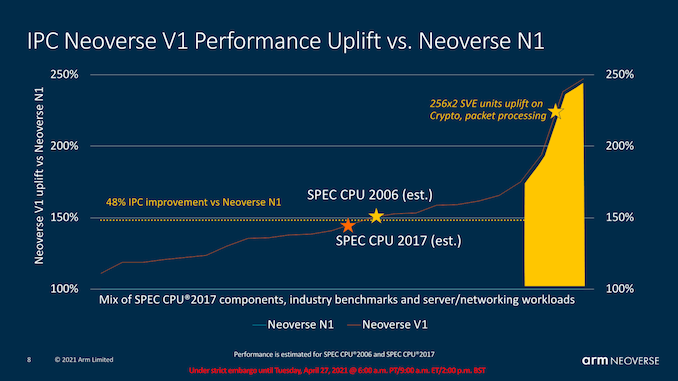
For the V1, the IPC improvements are roughly 50% median, with SPEC CPU essentially ending up at this figure. Arm made emphasis that there’s a set of workloads that are able to take advantage of SVE and the increased vector execution width of the V1 microarchitecture to achieve IPC improvements in excess of 100-125%, which is quite impressive.
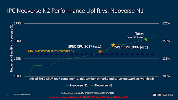
The N2’s median IPC increase lands at a median of 32%, with SPEC CPU at roughly those marketed 40% figure. The high-end isn’t as high as that of the V1, but still in excess of +50% IPC.
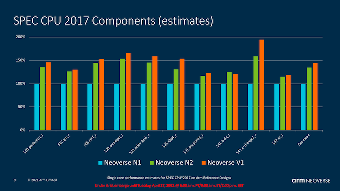
Finally, Arm also posted estimated figures for the components of SPEC CPU 2017, where we see the generational improvements be relatively even across the workloads, with a few exceptions where the V1’s larger characteristics come into play. There’s also workloads such as 541.leela_r where the N2 actually leads the V1, and Arm explained this by the fact that the N2 is actually a newer microarchitecture with further front-end improvements that aren’t found on the V1.
The CMN-700 Mesh Network - Bigger, More Flexible
It’s been a whole 5 years since we last wrote about Arm’s Coherent Mesh Network, the current generation CMN-600. The IP was announced quite some time ago, but has been a mainstay of Arm’s infrastructure IP for some time now, with it seeing some iterations in terms of IP revisions, with r2 introducing some important changes such as larger caches and CCIX capability.
Along with the V1 and N2, Arm today is also announcing a new generation CMN product in the form of the new CMN-700, promising much larger improvements to how Arm’s mesh network operates and what it is capable of in terms of scalability, performance, and flexibility.
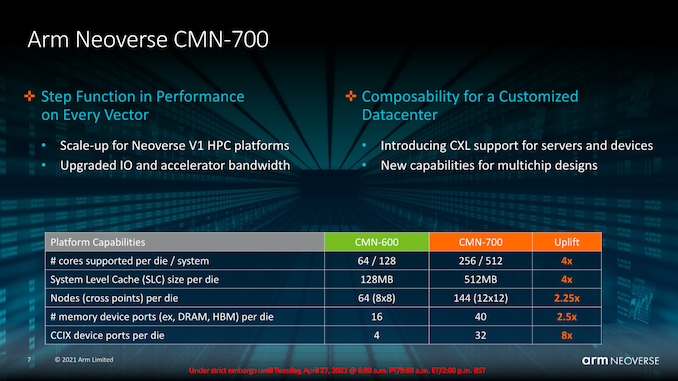
Starting off with the basic characteristics of the new design, the important big new feature is the fact that the mesh now has grown from a limit of 8 x 8 nodes (64) to 12 x 12 (144), allowing Arm to increase the number of CPUs on a single mesh and silicon die.
Terminology:
- RN-F: Fully coherent Request Node – Typically a CPU core, a CAL with two cores, or a DSU cluster
- HN-F: Fully coherent Home Node – A block of SLC cache with Snoop Filter
- CAL: Component Aggregation Layer – A block that houses two CPU cores connecting to one RN-F port
The actual maximum number of cores in a mesh has grown from 64 to 256, the latter number achievable through 128 RN-F request nodes each with 2 cores through a CAL (Component Aggregation Layer). For attentive readers, it might be weird to see Arm say that the CMN-600 only supports up to 64 cores when we have 80-core designs such as the Altra out there. Arm explained that the 64-core limit is through native cores connected to RN-F’s or through CALs, and that it’s actually possible to host more cores when you integrate them into the mesh through DSU (DynamiQ Shared Units). Ampere never confirmed their mesh layout, but this seems to be the only explanation of how they’d achieve a core count that high on the CMN-600.
Alongside 128 RN-Fs, hosting up to 256 cores, the chip hosts up to 128 HN-F home nodes, meaning nodes in which the SLC (System Level Cache) resides. Arm here discloses a maximum SLC of up to 512MB per die, meaning 4MB per node, while oddly enough saying the CMN-600 only supports 128MB, which technically is incorrect given that the reference manual says it goes up to 256MB at 4MB per node at 64 nodes.
In both cases, the SLC figures are a bit extreme and one shouldn’t expect designs with such sizes anytime soon.
Current generation Graviton2 and Altra Q chips only features 32MB SLC cache capacities in their mesh designs. One reason for this that in the past we haven’t talked about is that beyond the actual SLC, the HN-F nodes in the mesh also contain snoop filter caches that have particularly high size requirements. Arm states that generally the snoop filters need to be at least 1.5x the size of the aggregate exclusive caches of the cores, so in the case of the Altra Q with 80 cores and 1MB L2’s per core, that’s at least 120MB of required snoop filters caches on the mesh, alongside the 32MB of SLC. This would be very well a possible explanation as to why the SLCs are so small compared to say what AMD and Intel employ – the former for example using shadow tags of the L2’s for coherency (And the IOD having shadow tags of the CCD L3’s). It seems Arm’s design here is less area efficient.
The maximum memory controller (CHI SN-F nodes) in the mesh has been greatly increased from 16 to 40 ports, as Arm envisions more expansive mixed memory system architectures and designs to be employed in these newer designs.
Finally, CCIX ports have also seen a massive increase from 4 to 32, critical for some of the disaggregated chiplet designs that are also expected to be deployed – more on that in a bit.
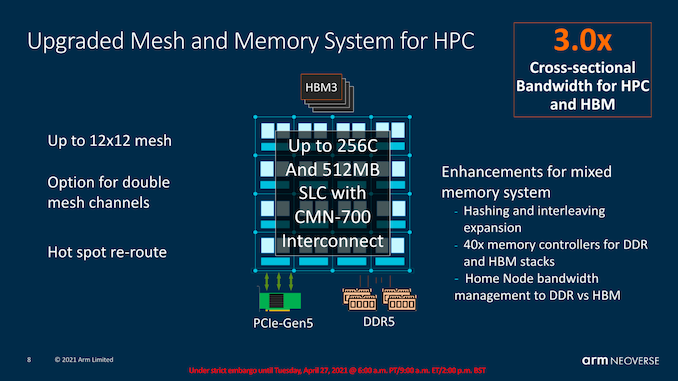
In terms of the memory capabilities, we noted that Arm expects hybrid architecture designs which would employ not only many more DDR memory controllers, but also integrate HBM memory. SiPearl’s Rhea chip is again such a confirmed design with 4x HBM2E stacks and 4-6 DDR5 memory controllers. The CMN-700 would be able to deal with such memory arrangements and properly manage the bandwidth and traffic across the heterogenous memory architectures.
Arm quotes a 3x increase in cross-sectional bandwidth in the mesh. Part of this is achieved through generational higher mesh frequencies, but the new design also most importantly now allows for doubled mesh channels between nodes. A mesh channel is still 256b wide with dedicated read and write ports, so a doubled-up design is essentially 2x256b in each direction. Arm discloses mesh frequencies of around 2GHz, so a 12x12 mesh with doubled up channels, if my math isn’t wrong, would result in cross-sectional bandwidth of around 3TB/s.
We asked Arm if the new mesh would be capable of more exotic 3D routing in terms of the direct interconnections between the nodes, but alas for this generation it’s still “only” limited to a 2D layout.
As noted in the V1 system features, CBusy is a new CPU-Mesh feature to alleviate mesh traffic congestions under high load, varying the CPU’s traffic requirements. There’s also general traffic improvements such as combining operations to reduce operations, or straightforward operations such as data-less writes to pages (Writing a page to all 0’s can be done with only one transaction, instead of writing zero to each cache line).
MPAM, again as explained in the earlier CPU section, helps traffic managing across independent workloads on a system such as VMs, ensuring QoS for SLA requirements, and general resource allocations across the entities in the system.
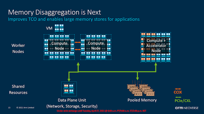
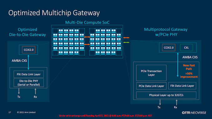
The CMN-600 this generation already had support for CCIX 1.1, which had been employed in designs such as the Altra Q. The CMN-700 now also introduces CCIX 2.0, as well as CXL compatibility.
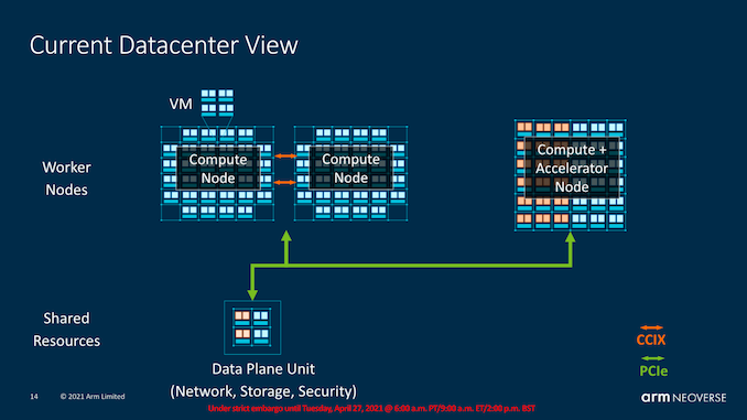
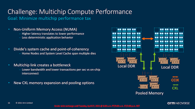
Besides operating with coherent accelerators over PCIe, Arm also sees memory disaggregation being a thing in the future, where we would see large pools of memory addressable by both the CPU clusters as well as the compute or accelerator nodes in a coherent fashion.
CCIX 2.0 is important for future multi-die and multi-socket designs as it’s allowed to get rid of the PCIe transaction and physical layers for a more closed generic link layer and PHY. One big disadvantage of the previous generation implementation, for example in multi-socket systems, was that it had tremendous latency penalties to cross all these different layers and protocols. We’ve seen the effect of this in our core-to-core test in the review of the Ampere Altra where the chip fared terribly in this regard.
The new CMN-700 and CCIX 2.0 connectivity promises to solve those very high latencies as well as the behaviour of requesting a remote socket cache line when talking between two cores in a local socket. This is not only important for socket-to-socket communications but also directly applies to chiplet-to-chiplet designs. It’s to be noted that Arm designs here still have to translate between AMBA CHI and CCIX 2.0 for such traffic, and whilst it’s much improved to what we’ve seen in the CCIX 1.1 implementations, it’s likely still not to be quite as performant as fully native protocol handling as for example Intel and AMD solutions.
In multi-chip systems where there’s a disaggregation of memory through NUMA domains can result in performance hits when working on the same data. An alleviation of such scenarios is the division of the home node coherency across two chips (This is why the CMN-700 is advertised as up to 512 cores in a “system”). This has disadvantages as the multi-chip link can create a bottleneck, but then it’s also possible to architect exotic designs such as having pooled memory with equal access between two chips.
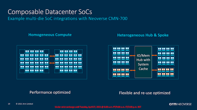
By now most readers will be familiar with AMD’s chiplet approach, and it’s a general architecture most vendors are heading towards given the slow-down of Moore’s law. Arm’s CMN-700 also allows for designs that are eerily similar to what AMD uses today, where a system can have a central IO Hub along with auxiliary compute dies.
We can have more traditional chip designs simply interconnected to each other, or more exotic designs with possible heterogenous chiplet architectures.
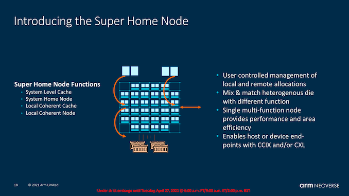
In the latter, Arm introduces the notion of a “Super Home Node” which acts as the central coherency point. In essence, this is simply just another mesh, but in theory it could be operated with no cores and simply just house an SLC (or none), and the central snoop filter handling coherency across all cores. In such an architecture, the SLC within that die would act as an L4 while the SLC in the mesh of a chiplet would act as an L3. There’s a bit of a mish-mash in terms of terminology here as we’re adding layers and chiplets, but I hope most will understand the hierarchy.
Eventual Design Performance Projections
Alongside the ISO-process node IPC, power and area projections, Arm also made projection of possible eventual implementations of the V1 and N2. These would naturally no longer be ISO-process, but the company’s expectations of what actual possible products might end up as in future designs.
The most important slide and disclosure in this regard is the fact that a Neoverse N2 design on TSMC’s 5nm is expected to achieve the same power as well as the same area as a TSMC 7nm Neoverse N1 design today.
In general, that’s a relatively large presumption, but could possibly pan out if the vendors are able to achieve a good implementation. We don’t have too many details as to the 7nm node generation of Amazon’s or Ampere’s current N1 chips, but I would assume that they’re baseline N7 – at least similar to that of what AMD uses in their EPYC 7002 and 7003 chips.
Still, a -40% power reduction from N7 to N5 is a very high goal and assumption to make. The only N5 chips we’ve had in-house to date, the Kirin 9000, and Apple A14, showcased only a rough 10% efficiency advantage over their N7P predecessors. N7P being roughly 15% better than N7, that’s still only somewhat 26% better efficiency.
Arm expects that the current generation N1 implementations to day to not have fully achieved their potential as it was the vendor’s first attempt with the IP. Arm expects that the following generations with more experience, better implementations with for example more metal layers, to be able to squeeze out more performance and power efficiency on the N5 node.
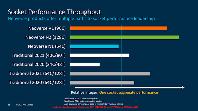
In terms of socket performance, Arm is expecting some very large generational gains versus a 64C N1 product today – it’s to be noted that these are Arm pre-silicon figures and not the Graviton2.
The “Traditional 2020” chips are the 24C Xeon 8268 and the 64C EPYC 7742. I would ignore the “Traditional 2021” parts here – Arm was aiming and estimating the performance of Intel’s newest 40C Ice-Lake and 64C Milan, however the presentation and figures here were integrated before AMD and Intel actually launched those systems – we have actual benchmark numbers in a custom graph below.
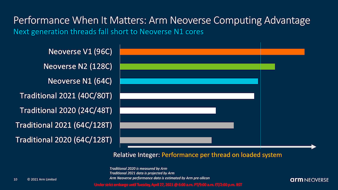
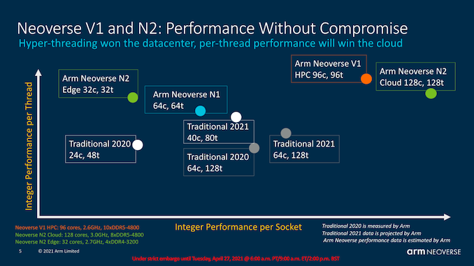
One metric Arm was focusing on was per-thread performance, where the “traditional” cores from AMD and Intel are falling short of the performance of Arm’s Neoverse cores.
Arm here is being somewhat sneaky in their presentation as they are trying to only focus on per-thread performance in cloud environments, where typically things operate on a vCPU basis, and essentially SMT-enabled designs from AMD and Intel naturally fall behind quite a lot in per-thread performance.
I can’t really blame Arm for depicting the performance figures like this – the cloud vendors today don’t really differentiate between real cores and SMT cores in vCPU environments, even having pricing that’s arguably unfair to SMT-enabled designs, which is why we’ve deemed Amazon’s Graviton2 m6g instances to vastly outperform AMD and Intel instances in terms of perf/W and perf/thread.
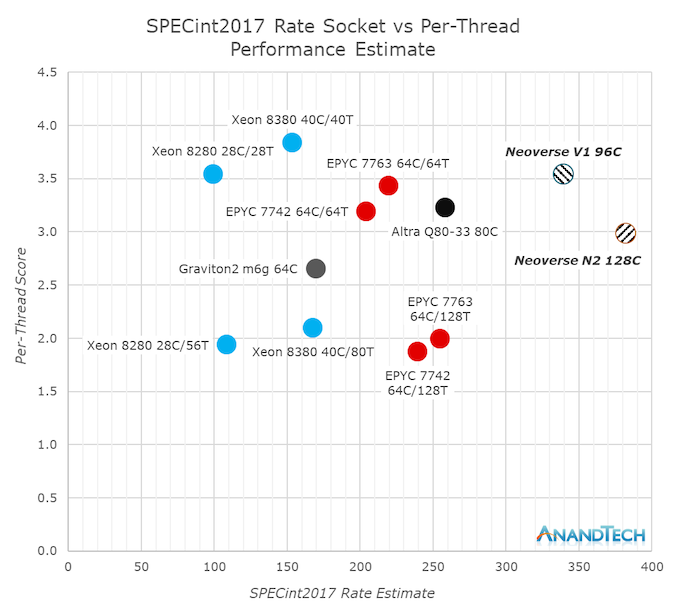
I wasn’t happy with Arm’s slides not including 1 thread per core performance figures for the SMT systems, so I included my own chart based on actual measured performance figures on the various platforms. The V1 and N2 figures use Arm’s performance scaling versus the Neoverse N1 datapoint, and I’ve baselined that to the Graviton2 scores we’ve measured earlier last year. Arm uses the same compiler flags as we do and also GCC 10.2, so the scores should also be compatible – with the only discrepancy being that Arm used 2MB page sizes.
The Neoverse V1 system uses 96 cores at 2.7GHz with 1MB L2 per core, on a 128MB 2GHz mesh, with 8 DDR5-4800 memory controllers. The N2 datapoint uses 128 3GHz cores at 1MB per L2, 96MB 2GHz mesh, with 10 DDR5-4800 memory controllers.
Arm’s per-thread performance lead doesn’t look that great here when looking at the 1T/C figures of AMD and Intel, but admittedly when in a vCPU scenario, Arm’s design would vastly outperform the SMT chips.
Generally speaking, the performance figures look good when it comes to per-socket performance, but generally that’s to be expected given the new 5nm process node and the more advanced memory controller technology in the projected figures.
AMD's next-generation Genoa should feature more massive performance jumps through the adoption of N5, DDR5, and transition away from their 14nm IO die. IPC and core count increases should also close the gap that’s depicted today. Intel’s next generation Sapphire Rapids should also improve the situation – albeit how that ends up depends on how much they’ll be able to squeeze out of 10nm SuperFin node in relation to what we’ve seen a few weeks ago on Ice Lake-SP.
Usually, I’m more open to Arm’s performance projections, however this time around the V1 and N2’s performance projections are extremely optimistic, especially since they’re completely dependent on the vendors achieving good implementations on N5 and actually reaching the projected 40% perf/W process node and implementation power efficiency gains. Based on what I’ve seen in the mobile space, I remain quite sceptical, and will be adopting a wait & see approach this time around.
First Thoughts & End Remarks
2020 was indeed a super-exciting year for Arm’s server ambitions, and one can easily claims that then Neoverse N1 has been a resounding success and implementations can be seen as being on the same playing field as the best that AMD and Intel are able to achieve, even against today’s newest generations.
The new Neoverse V1 and N2 continue the story in a 2-prong approach. For the Neoverse V1, back when the design was initially teased back in September, I was quite amazed at the claim of +50% IPC. After today’s figures, while the design is still very impressive, the disclosures of the power, area, and resulting power efficiency requirements have somewhat dulled my expectation of the new CPU microarchitecture.
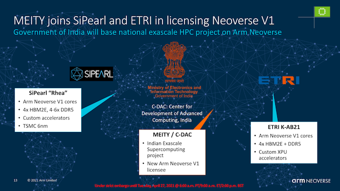
What’s clear about the Neoverse V1 is that this seems to really be an HPC-oriented design. Alongside the known SiPearl Rhea chip, backed by the European Processor Initiative’s goals for HPC uses, Korea’s ETRI (Electronics and Telecommunications Research Institute) also has a V1 designed dubbed “K-AB21” in the works, also with hybrid HBM2E and DDR5 memory. Along with today’s announcement of the V1, India’s Center for Development of Advanced Computing has also announced that they’re a V1 licensee and be using it in an exascale supercomputer project.
Essentially, it seems the V1 will serve as the foundation of many new custom HPC projects, which is a great win both for Arm as an IP vendor, as well as their licensees which are able to build something to their exact needs.
For enterprise and cloud usages, given the CPU’s power efficiency, I now doubt that we’ll somehow see implementations from cloud or merchant silicon vendors such as Amazon or Ampere, particularly because the N2 will be available.
The Neoverse N2 is a more straightforward migration from the N1. IPC is improved by significant amounts which should result in good generational performance increases. I have concerns about power efficiency as the performance increases come at a linear cost of increased power. There’s a one-time opportunity to increase performance in many workloads by closing the power-gap for workloads which do not fully fill the TDP of a system today (while throttling others), however any further performance increases beyond that are dependent on actual good physical implementations by the vendors to fully take advantage of the next-generation process nodes and to execute on those theoretical gains. We’ll see how that will pan out – for now I’ll give the Arm the benefit of doubt, however we’ll also see similar gains in 5nm designs from the likes of AMD. How the competitive situation will end up in 2022 remains to be seen.
Arm had also made a note that while the N2 is a newer generation IP than the V1, roughly a year apart in design, the company actually expects for N2 products to come out only shortly after V1 products, sometime by end of this year. This further enforces my view that we’ll probably not see much V1 designs outside of the HPC market, and that Amazon and Ampere are likely to follow up with N2 based Gravitons and Altras. I want to be explicit here that none of the usual cloud vendors / CSPs / hyperscalers have yet officially commented on what kind of IP they'll be using in the next-generation designs.
The star of the show today was I think the CMN-700, and the vast new flexibility it allows vendors to achieve. The new architectural improvements and the move towards CCIX 2.0 and CXL are definitive big advances that will allow licensees to create more exotic designs. At the very least, it allows for effective usage of chiplet architecture designs, which is a much-needed feature that vendors need to adopt to be able to ensure affordability and manufacturability of products on leading edge nodes.
I’ll be looking forward to new V1 and N2 designs in 2022, and hope we’ll hear more details from licensees through the course of the year.

