Stepping to the beat of a different drummer
The K6-2 is now available in a few new models or steppings as they are commonly referred to in the microprocessor industry. AMD just recently released three new additions to the K6-2 processor family, the K6-2 366, 380, and 400. The 366 and 380MHz parts are labeled Model 8/[7:0] as will all newer 350MHz parts, however the 400MHz unit is marked as a Model 8/[F:8] to indicate the use of AMD's new CXT core.
There have been reports of newer 350MHz parts with the newly improved core found in the 400MHz part, while older 350MHZ K6-2's are making use of the more common core found in the 7:0 processors...but what are the differences between these two processor revisions?
New Clock Multipliers
According to AMD's specifications, the K6-2 400 (Model 8/[F:8]) translates the 2.0x clock multiplier into a 6.0x clock multiplier as is defined by the below found in the AMD processor documentation
| State of BF[2:0] Inputs | Processor-Clock to Bus-Clock Ratio |
| 100b | 2.5x |
| 101b | 3.0x |
| 110b | 2.0x or 6.0x |
| 111b | 3.5x |
| 000b | 4.5x |
| 001b | 5.0x |
| 010b | 4.0x |
| 011b | 5.5x |
| The ratio selected is dependent on the stepping of the Model 8. The 2.0x ratio is supported on the Model 8/[7:0], whereas the 6.0x ratio is supported on the Model 8/[F:8]. | |
What does this mean? It basically indicates that stepping 7:0 of the model 8 K6-2 processor supports clock multipliers ranging from 2.0x - 5.5x, whereas stepping F:8 supports clock multipliers ranging from 2.5x - 6.0x, with the 2.0x setting corresponding to a 6.0x clock multiplier.
Why on earth would we need a 6.0x clock multiplier? For users that don't have Super7 motherboards, the K6-2 400 is still capable of running on your system, albeit considerably slower, at 66MHz x 6.0 instead of forcing it to run at 66MHz x 5.5. You'll begin to see more K6-2 overdrive type processors using the K6-2 400 as they can make use of the 6.0x clock multiplier to get the processor to work on motherboards that only support the 66MHz FSB.
Intolerable Heat
In addition to the new clock multiplier present in the F:8 chip, the 400MHz K6-2 also has a lower tolerance for an operating case temperature under maximum thermal power in comparison to previous parts, including other model 8 processors. Where the K6-2 350, 366, and 380MHz parts will allow for an ambient case temperature in the 00C–700C range, the 400MHz part is a bit more sensitive only allowing for a 00C–600C range. While this may not seem like a big problem considering your case shouldn't be in that range, in AnandTech's tests, the K6-2 400 seemed to be much more sensitive to thermal fluctuation than the K6-2 350 or 333. Some of that sensitivity can be attributed to the fact that AnandTech tested an engineering sample of the processor, however overall, you can expect the K6-2 400 to be a bit more sensitive to heat than its predecessors.
Write Handling Control Register
If you remember back to the release of the original AMD K6, one of the performance enhancing features that needed to be supported by motherboard manufacturers in their BIOS's on K6 compliant boards was "Write Allocate." Write allocate is a feature of the K6 architecture that allows the processor to cache a memory write that isn't already located within the L1 data cache. Using a burst read to fetch the data located outside the L1 cached region, a write allocate will store the data from the memory write in the processor's L1 data cache. Although the performance of a single write allocate function isn't greater than if the data were written to memory had a burst read not taken place, the real benefit of write allocate is visible in writes to the write allocated cache line after the initial write allocate. This is because the probability that a memory write will occur closer to a previous write is greater than a memory write occurring in an area far away from the previous write. Eventually, you'll experience a performance gain from using multiple write allocates in comparison to forgoing the burst read cycles and allowing the memory writes to complete without write allocate intervention.
Write allocate can be triggered via one [or more] of three methods that indicate an "eligible" memory write is taking place: Write to a Cacheable Page, Write to a Sector, and Write Allocate Limit. The main difference between the two steppings of the model 8 K6-2 discussed here occurs in the usage of the Write Allocate Limit method. The Write Allocate Limit is enabled by what is known as the Write Handling Control Register, or WHCR for short.
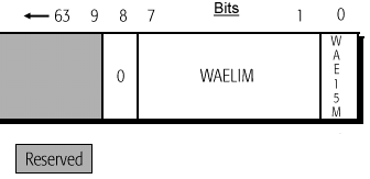
In stepping 7:0 of K6-2 processors, the WHCR is composed of three fields: the WCDE bit, the Write Allocate Enable Limit (WAELIM) field, and the Write Allocate Enable 15-to-16Mbyte (WAE15M) bit as described by the following figure taken from AMD's K6-2 400 documentation:
Stepping F:8 changes the picture slightly, with the WHCR composed of two fields: the Write Allocate Enable Limit (WAELIM) field, and the Write Allocate Enable 15-to-16Mbyte (WAE15M) bit as described by the following figure taken from AMD's K6-2 400 documentation:
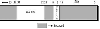
One thing you'll notice is that the WAELIM field is larger in the second diagram (10 bits wide - Model 8/[F:8]) in comparison to the first diagram (7 bits wide - Model 8/[7:0]). This indicates that the theoretical limit for Write Allocates to take place in the F:8 stepping has been raised from 508MB of memory to 4096MB as was the case with older processors. Once again, we have been given a feature that really won't effect us that much, however the real performance increase comes from the next enhancement which somewhat walks hand in hand with Write Allocate.
Write Merge Buffer
Where Write Allocate fails, the K6-2's (Model 8/[F:8]) 8-byte Write Merge Buffer picks up. Instead of simply leaving non-cacheable write cycles alone, the Write Merge Buffer combines the data segments from all a group of memory writes into this 8-byte buffer. By combining all of the writes into the Write Merge Buffer, you can theoretically reduce processor bus utilization and processor stalls, which accounts for the overall increase in performance the newer F:8 stepping offers over the older processors.


0 Comments
View All Comments