3D Packaging

Under the CHIPS & Science Act, the U.S. government provided tens of billions of dollars in grants and loans to the world's leading maker of chips, such as Intel, Samsung, and TSMC, which will significantly expand the country's semiconductor production industry in the coming years. However, most chips are typically tested, assembled, and packaged in Asia, which has left the American supply chain incomplete. Addressing this last gap in the government's domestic chip production plans, these past couple of weeks the U.S. government signed memorandums of understanding worth about $1.5 billion with Amkor and SK hynix to support their efforts to build chip packaging facilities in the U.S. Amkor to Build Advanced Packaging Facility with Apple in Mind Amkor plans to build a $2 billion advanced...
TSMC's 3D Stacked SoIC Packaging Making Quick Progress, Eyeing Ultra-Dense 3μm Pitch In 2027
TSMC's 3D-stacked system-on-integrated chips (SoIC) advanced packaging technologies is set to evolve rapidly. In a presentation at the company's recent technology symposium, TSMC outlined a roadmap that will take...
1 by Anton Shilov on 5/31/2024
TSMC Readies 8x Reticle Super Carrier Interposer For Next-Gen Chips Twice as Large As Today's
TSMC is no stranger to building big chips. Besides the ~800mm2 reticle limit of their normal logic processes, the company already produces even larger chips by fitting multiple dies...
6 by Anton Shilov on 4/30/2024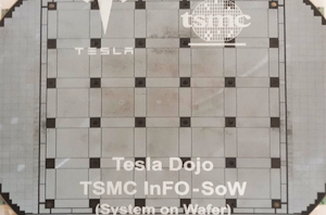
TSMC's System-on-Wafer Platform Goes 3D: CoW-SoW Stacks Up the Chips
TSMC has been offering its System-on-Wafer integration technology, InFO-SoW, since 2020. For now, only Cerebras and Tesla have developed wafer scale processor designs using it, as while they have...
2 by Anton Shilov on 4/26/2024
Amkor to Build $2 Billion Chip Packaging Fab in Arizona Primarily for Apple
Amkor, the world's second largest independent outsourced semiconductor assembly and test (OSAT) service provider, has announced their intention to build a new advanced chip packaging facility in the U.S...
12 by Anton Shilov on 12/4/2023
TSMC: Short Supply of HPC GPUs to Persist for 1.5 Years
The reports about an insufficient supply of compute GPUs used for artificial intelligence (AI) and high-performance computing (HPC) servers became common in recent months as demand for GPUs to...
6 by Anton Shilov on 9/7/2023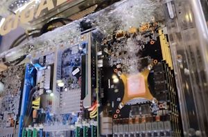
As HPC Chip Sizes Grow, So Does the Need For 1kW+ Chip Cooling
One trend in the high performance computing (HPC) space that is becoming increasingly clear is that power consumption per chip and per rack unit is not going to stop...
40 by Anton Shilov on 6/27/2022_carousel.jpg)
Intel Accelerated Webcast on July 26th: Update on Process Technology and Roadmaps
Earlier this year, new Intel CEO Pat Gelsinger outlined his new ‘IDM 2.0’ vision for Intel. This vision was a three pronged strategy based on improving its own process...
32 by Dr. Ian Cutress on 7/12/2021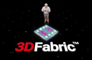
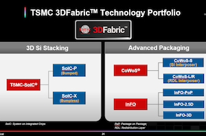
3DFabric: The Home for TSMC’s 2.5D and 3D Stacking Roadmap
Interposers. EMIB. Foveros. Die-to-die stacking. ODI. AIB.TSVs. All these words and acronyms have one overriding feature – they are all involved in how two bits of silicon physically connect...
9 by Dr. Ian Cutress on 9/2/2020_carousel.jpg)
Intel Next-Gen 10-micron Stacking: Going 3D Beyond Foveros
One of the issues facing next-generation 3D stacking of chips is how to increase the density of the die-to-die interface. More connections means better data throughput, reducing latency and...
32 by Dr. Ian Cutress on 8/14/2020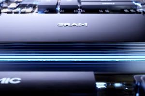
Samsung Announces "X-Cube" 3D TSV SRAM-Logic Die Stacking Technology
Yesterday, Samsung Electronics had announced a new 3D IC packaging technology called eXtended-Cube, or “X-Cube”, allowing chip-stacking of SRAM dies on top of a base logic die through TSVs. Current...
21 by Andrei Frumusanu on 8/14/2020


