GAAFET

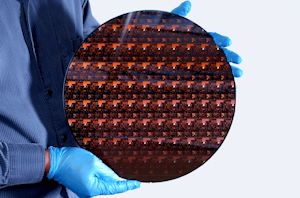
This week Samsung Electronics and Synopsys announced that Samsung has taped out its first mobile system-on-chip on Samsung Foundry's 3nm gate-all-around (GAA) process technology. The announcement, coming from electronic design automation Synopsys, further notes that Samsung used the Synopsys.ai EDA suite to place-n-route the layout and verify design of the SoC, which in turn enabled higher performance. Samsung's unnamed high-performance mobile SoC relies on 'flagship' general-purpose CPU and GPU architectures as well as various IP blocks from Synopsys. SoC designers used Synopsys.ai EDA software, including the Synopsys DSO.ai to fine-tune design and maximize yields as well as Synopsys Fusion Compiler RTL-to-GDSII solution to achieve higher performance, lower power, and optimize area (PPA). And while the news that Samsung has developed a high-performance SoC using the Synopsys.ai...
Rapidus Wants to Supply 2nm Chips to Tech Giants, Challenge TSMC
It has been a couple of decades since a Japanese fab has offered a leading-edge chip manufacturing process. Even to this day, none of the Japanese chipmakers have made...
19 by Anton Shilov on 7/26/2023
GlobalFoundries Sues IBM Over Sharing Leading-Edge Chip IP with Intel, Rapidus
The relationship between GlobalFoundries and IBM has been rocky in recent years. Among other things, Big Blue has previously sued GF, seeking damages for abruptly stopping the development of...
10 by Anton Shilov on 4/20/2023
Samsung Starts 3nm Production: The Gate-All-Around (GAAFET) Era Begins
Capping off a multi-year development process, Samsung’s foundry group sends word this morning that the company has officially kicked off production on its initial 3nm chip production line. Samsung’s...
22 by Ryan Smith on 6/30/2022
TSMC: N2 To Start With Just GAAFETs, Add Backside Power Delivery Later
When TSMC initially introduced its N2 (2 nm class) process technology earlier this month, the company outlined how the new node would be built on the back of two...
16 by Anton Shilov on 6/29/2022
Intel’s First High-Profile IFS Fab Customer: Qualcomm Jumps on Board For 20A Process
Alongside Intel’s sizable announcement today regarding their manufacturing roadmap over the next half-decade, the company is also announcing their first major customer for their third-party foundry service, IFS. And...
59 by Ryan Smith on 7/26/2021
Samsung: Deployment of 3nm GAE Node on Track for 2022
Samsung Foundry has made some changes to its plans concerning its 3 nm-class process technologies that use gate-all-around (GAA) transistors, or what Samsung calls its multi-bridge channel field-effect transistors...
32 by Anton Shilov on 7/9/2021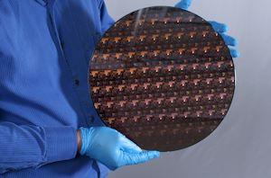
IBM Creates First 2nm Chip
Every decade is the decade that tests the limits of Moore’s Law, and this decade is no different. With the arrival of Extreme Ultra Violet (EUV) technology, the intricacies...
118 by Dr. Ian Cutress on 5/6/2021
TSMC to Spend $100B on Fabs and R&D Over Next Three Years: 2nm, Arizona Fab & More
TSMC this week has announced plans to spend $100 billion on new production facilities as well as R&D over the next three years. The world's largest contract maker of...
45 by Anton Shilov on 4/2/2021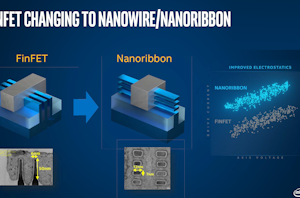
Intel to use Nanowire/Nanoribbon Transistors in Volume ‘in Five Years’
This year, at the international VLSI conference, Intel’s CTO Mike Mayberry gave one of the plenary presentations, which this year was titled ‘The Future of Compute’. Within the presentation...
14 by Dr. Ian Cutress on 6/22/2020_carousel.jpg)
Samsung Announces 3nm GAA MBCFET PDK, Version 0.1
So what comes after 7nm, after 6nm, after 5nm, and after 4nm? That's right: 3nm! At Samsung's Foundry Forum event today, Samsung has announced that the first alpha version...
32 by Dr. Ian Cutress on 5/14/2019
Samsung Foundry Roadmap: EUV-Based 7LPP for 2018, 3 nm Incoming
Samsung Foundry this week updated its fabrication technology roadmap, introducing a number of changes and announcing the first details about its 3 nm manufacturing process that is several years...
25 by Anton Shilov on 5/24/2018


