AMD 7th Gen Bristol Ridge and AM4 Analysis: Up to A12-9800, B350/A320 Chipset, OEMs first, PIBs Later
by Ian Cutress on September 23, 2016 9:00 AM EST
Over the last two weeks, AMD officially launched their 7th Generation Bristol Ridge processors as well as the new AM4 socket and related chipsets. The launch was somewhat muted, as the target for the initial launch is purely to the big system OEMs and system integrators, such as Lenovo, HP, Dell and others – for users wanting to build their own systems, ‘Product-in-Box’ units (called PIBs) for self-build systems will come at the end of the year. We held off on the announcement because the launch and briefings left a number of questions unanswered as to the potential matrix of configurations, specifications of the hardware and how it all connects together. We got a number of answers, so let’s delve in.
The CPUs
The seven APUs and one CPU being launched for OEM systems spans from a high-frequency A12 part using the 7th Generation microarchitecture (we call it Excavator v2) to the A6, and they all build on the Bristol Ridge notebook parts that were launched earlier in the year but focused on the desktop this time around. AMD essentially skipped the 6th Gen, Carrizo, for desktop as the design was significantly mobile focused – we ended up with one CPU, the Athlon X4 845 (which we reviewed), with DDR3 support but no integrated graphics. Using the updated 28nm process from TSMC, AMD was able to tweak the microarchitecture and allow full on APUs for desktops using a similar design.
The full list of processors is as follows:
| AMD 7th Generation Bristol Ridge Processors | |||||
| Modules/ Threads |
CPU Base / Turbo (MHz) |
GPU | GPU Base / Turbo (MHz) |
TDP | |
| A12-9800 | 2M / 4T | 3800 / 4200 | Radeon R7 | 800 / 1108 | 65W |
| A12-9800E | 2M / 4T | 3100 / 3800 | Radeon R7 | 655 / 900 | 35W |
| A10-9700 | 2M / 4T | 3500 / 3800 | Radeon R7 | 720 / 1029 | 65W |
| A10-9700E | 2M / 4T | 3000 / 3500 | Radeon R7 | 600 / 847 | 35W |
| A8-9600 | 2M / 4T | 3100 / 3400 | Radeon R7 | 655 / 900 | 65W |
| A6-9500 | 1M / 2T | 3500 / 3800 | Radeon R5 | 720 / 1029 | 65W |
| A6-9500E | 1M / 2T | 3000 / 3400 | Radeon R5 | 576 / 800 | 35W |
| Athlon X4 950 | 2M / 4T | 3500 / 3800 | - | - | 65W |
AMD’s mainstream processors will now hit a maximum of 65W in their official thermal design power (TDP), with the launch offering a number of 65W and 35W parts. There is the potential to offer CPUs with a configurable TDP, however much like the older parts that supported 65W/45W modes, it was seldom used, and chances are we will see OEMs stick with the default design power windows here. Also, the naming scheme: any 35W part now has an ‘E’ at the end of the processor name, allowing for easier identification.
As part of this review, we were able to snag a few extra configuration specifications for each of the processors, including the number of streaming processors in each, base GPU frequencies, base Northbridge frequencies (more on the NB later), and confirmation that all the APUs launched will support DDR4-2400 at JEDEC sub-timings.
| AMD 7th Generation 65W Bristol Ridge Processors | |||||
| Modules/ Threads |
CPU Base / Turbo (MHz) |
GPU SPs |
GPU Base / Turbo (MHz) |
Northbridge Base (MHz) |
|
| A12-9800 | 2M / 4T | 3800 / 4200 | 512 | 800 / 1108 | 1400 |
| A10-9700 | 2M / 4T | 3500 / 3800 | 384 | 720 / 1029 | 1400 |
| A8-9600 | 2M / 4T | 3100 / 3400 | 384 | 655 / 900 | 1300 |
| A6-9500 | 1M / 2T | 3500 / 3800 | 384 | 720 / 1029 | 1400 |
| Athlon X4 950 | 2M / 4T | 3500 / 3800 | - | - | 1400 |
| AMD 7th Generation 35W Bristol Ridge Processors | |||||
| Modules/ Threads |
CPU Base / Turbo (MHz) |
GPU SPs |
GPU Base / Turbo (MHz) |
Northbridge Base (MHz) |
|
| A12-9800E | 2M / 4T | 3100 / 3800 | 512 | 655 / 900 | 1300 |
| A10-9700E | 2M / 4T | 3000 / 3500 | 384 | 600 / 847 | 1300 |
| A6-9500E | 1M / 2T | 3000 / 3400 | 256 | 576 / 800 | 1300 |
The A12-9800 at the top of the stack is an interesting part on paper. If we do a direct comparison with the previous high-end AMD APUs, the A10-7890K, A10-7870K and A10-7860K, a lot of positives end up on the side of the A12.
| High-End AMD APU Comparison | |||||||
| A12-9800 | A10-7890K | A10-7870K | A10-7860K | A10-9700 | |||
| MSRP | - | $165 | $137 | $117 | - | ||
| Platform | Bristol Ridge | Kaveri Refresh | Bristol Ridge | ||||
| uArch | Excavator v2 | Steamroller | Steamroller | Steamroller | Excavator v2 | ||
| Threads | 2M / 4T | 2M / 4T | 2M / 4T | 2M / 4T | 2M / 4T | ||
| CPU Base Freq | 3800 | 4100 | 3900 | 3600 | 3500 | ||
| CPU Turbo Freq | 4200 | 4300 | 4100 | 4000 | 3800 | ||
| IGP SPs | 512 | 512 | 512 | 512 | 384 | ||
| GPU Turbo Freq | 1108 | 866 | 866 | 757 | 1029 | ||
| TDP | 65W | 95W | 95W | 65W | 65W | ||
| L1-I Cache | 192 KB | 192 KB | 192 KB | 192 KB | 192 KB | ||
| L1-D Cache | 128 KB | 64 KB | 64 KB | 64 KB | 128 KB | ||
| L2 Cache | 2 MB | 4 MB | 4 MB | 4 MB | 2 MB | ||
| DDR Support | DDR4-2400 | DDR3-2133 | DDR3-2133 | DDR3-2133 | DDR4-2400 | ||
| PCIe 3.0 | x8 | x16 | x16 | x16 | x8 | ||
| Chipsets | B350 A320 X/B/A300 |
A88X A78 A68H |
A88X A78 A68H |
A88X A78 A68H |
B350 A320 X/B/A300 |
||
The frequency of the A12-9800 gives it a greater dynamic range than the A10-7870K (having 3.8-4.2 GHz, rather than 3.9-4.1), but with the newer Excavator v2 microarchitecture, improved L1 cache, AVX 2.0 support and a much higher integrated graphics frequency (1108 MHz vs. 866 MHz) while also coming in at 30W less TDP. The 30W TDP jump is the most surprising – we’re essentially getting better than the previous A10-class performance at a lower power, which is most likely why they started naming the best APU in the stack an ‘A12’. Basically, the A12-9800 APU will be an extremely interesting one to review given the smaller L2 cache but faster graphics and DDR4 memory.
A Wild Overclocker Appears!
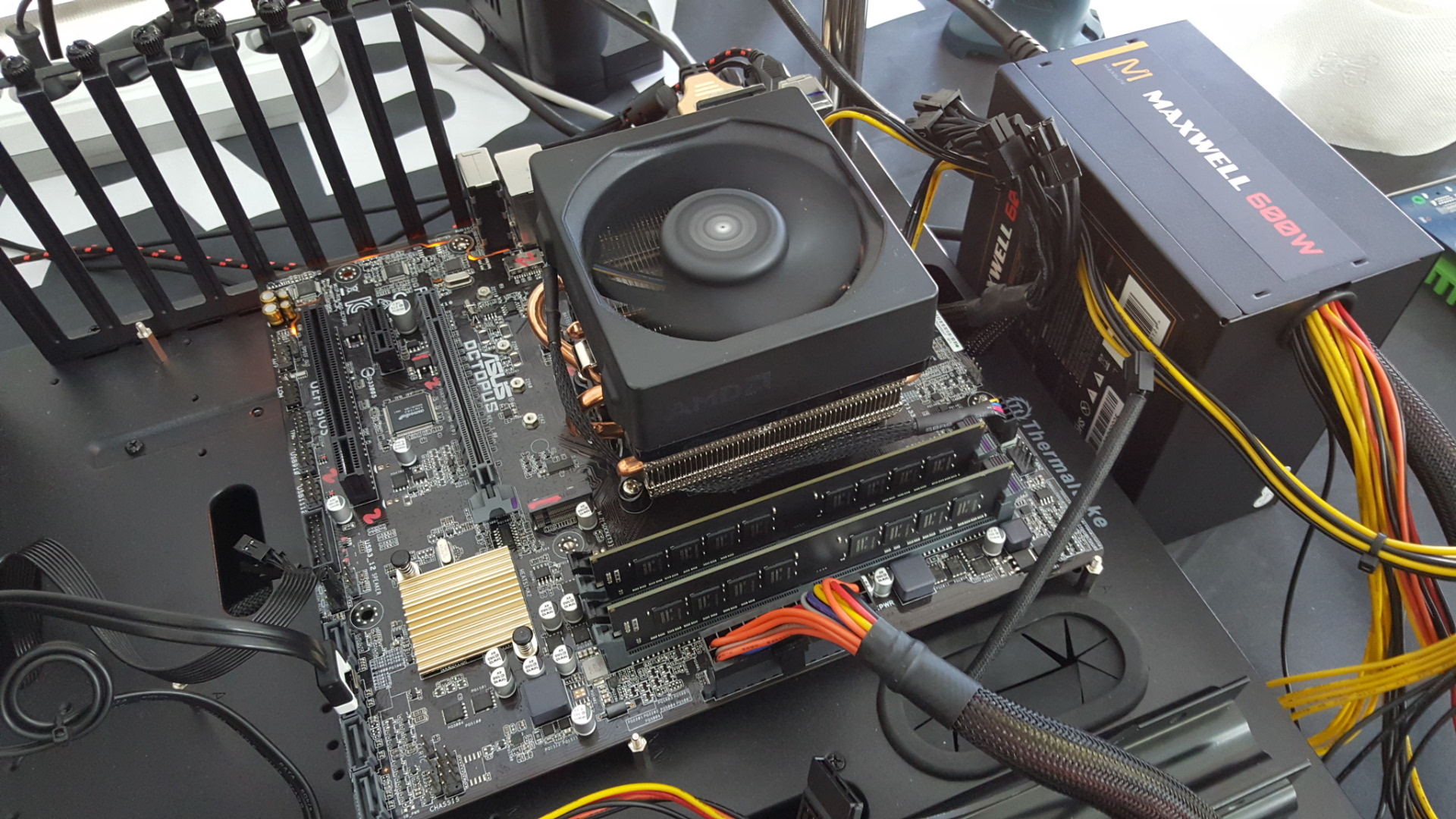
Given that technically the systems with the new APUs have been released for a couple of weeks, some vendors have their internal enthusiasts play around with the platform. Bearing in mind that AMD has not announced any formal overclocking support on these new APUs, NAMEGT, a South Korean overclocker with ties to ASUS, has pushed the A12-9800 APU to 4.8 GHz by adjusting the multiplier. To do this, he used an unreleased ASUS Octopus AM4 motherboard and AMD’s 125W Wraith air cooler (which will presumably be bundled with PIBs later in the product cycle).
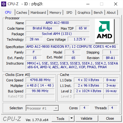
NAMEGT ran this setup on multithreaded Cinebench 11.5 and Cinebench 15, scoring 4.77 and 380 respectively for a 4.8 GHz overclock. If we compare this to our Bench database results, we see the following
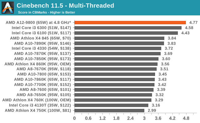
For Cinebench 15, this overclocked score puts the A12-9800 above the Haswell Core i3-4360 and the older AMD FX-4350, but below the newer Skylake i3-6100TE. The Athlon X4 845 at stock frequencies scored 314 while running at 3.5 GHz, which would suggest that a stock A12-9800 at 3.8 GHz would fall around the 340 mark.
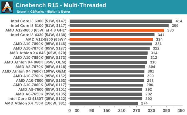
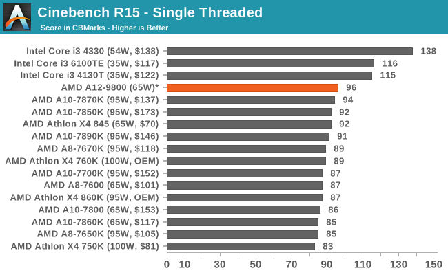
(Since writing this, a preview by Korean website Bodnara, using the A12-9800 in a GIGABYTE motherboard, scored 334 for a stock Cinebench 15 multithreaded test and 96 for the single threaded test. We've added this result for perspective.)
When we previously tested the Excavator architecture for desktop on the 65W Athlon X4 845, overclocking was a nightmare, with stability being a large issue. At the time, we suspected that due to the core design being focused towards 15W, moving beyond 65W was perhaps a bit of a stretch for the design at hand. This time around, as we reported before, Bristol Ridge is using an updated 28nm process over Carrizo, which may have a hand in this.
When we asked AMD about overclocking details on the new APUs, the return reply was along the lines of ‘No OEM systems at this time will be unlocked, and no official comment on the individual units. More details will be released closer to the platform launch for DIY users’.


122 Comments
View All Comments
patrickjp93 - Tuesday, September 27, 2016 - link
Yeah, no. Even the 5775C has thoroughly beaten everything AMD has so far offered, even if narrowly. Skylake GT3e increased that gap, and GT4e dug a canyon between Intel and AMD. This is why I sincerely doubt AMD's HPC APUs will get much traction.MrCommunistGen - Tuesday, September 27, 2016 - link
Skylake's GT4e really is in a whole new league of iGPU performance (at a significant cost) - but to nitpick GT3e on Skylake very likely underperforms GT3e on Broadwell.Broadwell GT3e (specifically Iris Pro 6200) is 48EUs at up to 1150MHz backed by 128MB eDRAM on a 65W TDP quad core.
Skylake GT3e (specifically Iris Graphics 550) is 48EUs at up to 1100MHz backed by 64MB eDRAM on a 28W dual core. (I'm not counting the listing for the "Server" GT3e which is listed as P555 with 128MB)
Skylake has microarchitecture improvements to both the EUs and to the x86 cores. It also supports DDR4 and Gen9 includes delta compression - so the iGPU undoubtedly has more bandwidth available.
That said, I really think that the smaller eDRAM, lower TDP, and lower max clock speed will make SKL GT3e slower than BDW GT3e.
Due to the rearrangement of SKUs and iGPUs in SKL I think this is all natural. Intel is trying to *significantly* increase the iGPU perf available to their 15/28W dual core CPUs with its iteration of GT3e, however this allows for the potential that this architecture's GT3e underperforms the previous.
Danvelopment - Saturday, September 24, 2016 - link
Something seems a bit funny about the IGPs of the A8 and A6. The A8 states R7 with 384SPs and a lower clock than the R5 in the A6 also with 384SPs.Should the A6 be R7 or 256 SPs? And if it's correct, how does the IGP compare between the two? And what makes the A8 faster?
Danvelopment - Saturday, September 24, 2016 - link
Also, any chance in getting a couple R5 performance indicators?MrCommunistGen - Tuesday, September 27, 2016 - link
I noticed that too. I've seen tables and slides from various sites and they all list those specs. The only thing I can conclude is that since the A6 has half the CPU resources, maybe AMD just assumes that for most tasks you'll end up CPU bound to a large enough degree that even thought the iGPU is technically faster, performance will be lower.Or... the alternative is that there's a typo of some sort in the original materials published by AMD.
yannigr2 - Saturday, September 24, 2016 - link
Oh, really nice article. Thanks for this.Well the first Zen processors will probably cost more than the A12. Then when Zen based APUs will be ready to come to the market, we will see and smaller Zen models.
ET - Saturday, September 24, 2016 - link
Thanks for the writeup, Ian. I even learned some new things which I haven't yet read elsewhere. I do hope that Anandtech can get its hands on a chip for reviews.NeatOman - Sunday, September 25, 2016 - link
Marginal improvement IMO over last gen APU's. Looks interesting but an i3 will still "feel" faster as its single core power is still greater, although i almost always build AMD APU's for small offices because Microcenter has a instant $40 rebate when you buy in store. BUT.. ZEN SoC with HBM might be a game changer (to quote 2014), and rumor is Apple is eyeballing it for the next Macbook Pro. And AMD has a good track record on Unix based OS's which might be why the Mac Pro uses AMD... I'm going down a rabbit hole. SOO! A12... ehh.. no significant change but I'm waiting for ZEN.utroz - Sunday, September 25, 2016 - link
Ian Cutress on the first page you say: "Using the updated 28nm process from TSMC, AMD was able to tweak the microarchitecture and allow full on APUs for desktops using a similar design."Problem is that Carrizo and Bristol Ridge are actually made at Global Foundries on a 28nm process.
TheinsanegamerN - Monday, September 26, 2016 - link
"Back at Computex, AMD announced the thing to fill that hole: Bristol Ridge (and Stoney Ridge by extension). This is what AMD will call and market it's '7th Generation' of APUs, and will be built on TSMC's 28nm Bulk CMOS process."From anandtech's look at carrizo in july. Everything else i've found doesnt say GF or TSMC, just 28nm.
so far, evidence is pointing at TSMC, not GF.