AMD 7th Gen Bristol Ridge and AM4 Analysis: Up to A12-9800, B350/A320 Chipset, OEMs first, PIBs Later
by Ian Cutress on September 23, 2016 9:00 AM ESTThe Integrated GPU
For all but one of the processors, integrated graphics is the name of the game. AMD configures the integrated graphics in terms of Compute Units (CUs), with each CU having 64 streaming processors (SPs) using GCN 1.3 (aka GCN 3.0) architecture, the same architecture as found in AMD’s R9 Fury line of GPUs. The lowest processor in the stack, the A6-9500E, will have four CUs for 256 SPs, and the A12 APUs will have eight CUs, for 512 SPs. The other processors will have six CUs for 384 SPs, and in each circumstance the higher TDP processor typically has the higher base and turbo frequency.
| AMD 7th Generation Bristol Ridge Processors | |||||
| GPU | GPU SPs | GPU Base | GPU Turbo | TDP | |
| A12-9800 | Radeon R7 | 512 | 800 | 1108 | 65W |
| A12-9800E | Radeon R7 | 512 | 655 | 900 | 35W |
| A10-9700 | Radeon R7 | 384 | 720 | 1029 | 65W |
| A10-9700E | Radeon R7 | 384 | 600 | 847 | 35W |
| A8-9600 | Radeon R7 | 384 | 655 | 900 | 65W |
| A6-9500 | Radeon R5 | 384 | 720 | 1029 | 65W |
| A6-9500E | Radeon R5 | 256 | 576 | 800 | 35W |
| Athlon X4 950 | - | - | - | - | 65W |
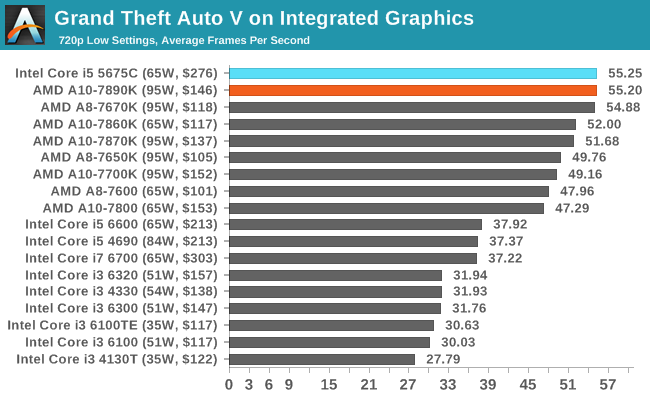
The new top frequency, 1108 MHz, for the A12-9800 is an interesting element in the discussion. Compared to the previous A10-7890K, we have a +28% increase in raw GPU frequency with the same number of streaming processors, but a lower TDP. This means one of two things – either the 1108 MHz frequency mode is a rare turbo state as the TDP has to be shared between the CPU and APU, or the silicon is sufficient enough to maintain a 28% higher frequency with ease. Obviously, based on the overclocking results seen previously, it might be interesting to see how the GPU might change in frequency without a TDP barrier and with sufficient cooling. For comparison, when we tested the A10-7890K in Grand Theft Auto at a 1280x720 resolution and low-quality settings, we saw an average 55.20 FPS.
Bearing in mind the change in the cache configuration moving to Bristol Ridge, moving from a 4 MB L2 to a 2 MB L2 but increasing the DRAM compatibility from DDR3-2133 to DDR4-2400, that value should move positive, and distinctly the most cost effective part for gaming.
Each of these processors supports the following display modes:
- DVI, 1920x1200 at 60 Hz
- DisplayPort 1.2a, 4096x2160 at 60 Hz (FreeSync supported)
- HDMI 2.0, 4096x2160 at 60 Hz
- eDP, 2560x1600 at 60 Hz
Technically the processor will support three displays, with any mix of the above. Analog video via VGA can be supported by a DP-to-VGA converter chip on the motherboard or via an external dongle.
For codec support, Bristol Ridge can do the following (natively unless specified):
- MPEG2 Main Profile at High Level (IDCT/VLD)
- MPEG4 Part 2 Advanced Simple Profile at Level 5
- MJPEG 1080p at 60 FPS
- VC1 Simple and Main Profile at High Level (VLD), Advanced Profile at Level 3 (VLD)
- H.264 Constrained Baseline/Main/High/Stereo High Profile at Level 5.2
- HEVC 8-bit Main Profile Decode Only at Level 5.2
- VP9 decode is a hybrid solution via the driver, using CPU and GPU
AMD still continues to support HSA and the arrangement between the Excavator v2 modules in Bristol Ridge and the GCN graphics inside is no different – we still get Full 1.0 specification support. With the added performance, AMD is claiming equal scores for the A12-9800 on PCMark 8 Home with OpenCL acceleration as a Core i5-6500 ($192 tray price), and the A12-9800E is listed as a 17% increase in performance over the i5-6500T. With synthetic gaming benchmarks, AMD is claiming 90-100% better performance for the A12 over the i5 competition.


122 Comments
View All Comments
patrickjp93 - Tuesday, September 27, 2016 - link
Yeah, no. Even the 5775C has thoroughly beaten everything AMD has so far offered, even if narrowly. Skylake GT3e increased that gap, and GT4e dug a canyon between Intel and AMD. This is why I sincerely doubt AMD's HPC APUs will get much traction.MrCommunistGen - Tuesday, September 27, 2016 - link
Skylake's GT4e really is in a whole new league of iGPU performance (at a significant cost) - but to nitpick GT3e on Skylake very likely underperforms GT3e on Broadwell.Broadwell GT3e (specifically Iris Pro 6200) is 48EUs at up to 1150MHz backed by 128MB eDRAM on a 65W TDP quad core.
Skylake GT3e (specifically Iris Graphics 550) is 48EUs at up to 1100MHz backed by 64MB eDRAM on a 28W dual core. (I'm not counting the listing for the "Server" GT3e which is listed as P555 with 128MB)
Skylake has microarchitecture improvements to both the EUs and to the x86 cores. It also supports DDR4 and Gen9 includes delta compression - so the iGPU undoubtedly has more bandwidth available.
That said, I really think that the smaller eDRAM, lower TDP, and lower max clock speed will make SKL GT3e slower than BDW GT3e.
Due to the rearrangement of SKUs and iGPUs in SKL I think this is all natural. Intel is trying to *significantly* increase the iGPU perf available to their 15/28W dual core CPUs with its iteration of GT3e, however this allows for the potential that this architecture's GT3e underperforms the previous.
Danvelopment - Saturday, September 24, 2016 - link
Something seems a bit funny about the IGPs of the A8 and A6. The A8 states R7 with 384SPs and a lower clock than the R5 in the A6 also with 384SPs.Should the A6 be R7 or 256 SPs? And if it's correct, how does the IGP compare between the two? And what makes the A8 faster?
Danvelopment - Saturday, September 24, 2016 - link
Also, any chance in getting a couple R5 performance indicators?MrCommunistGen - Tuesday, September 27, 2016 - link
I noticed that too. I've seen tables and slides from various sites and they all list those specs. The only thing I can conclude is that since the A6 has half the CPU resources, maybe AMD just assumes that for most tasks you'll end up CPU bound to a large enough degree that even thought the iGPU is technically faster, performance will be lower.Or... the alternative is that there's a typo of some sort in the original materials published by AMD.
yannigr2 - Saturday, September 24, 2016 - link
Oh, really nice article. Thanks for this.Well the first Zen processors will probably cost more than the A12. Then when Zen based APUs will be ready to come to the market, we will see and smaller Zen models.
ET - Saturday, September 24, 2016 - link
Thanks for the writeup, Ian. I even learned some new things which I haven't yet read elsewhere. I do hope that Anandtech can get its hands on a chip for reviews.NeatOman - Sunday, September 25, 2016 - link
Marginal improvement IMO over last gen APU's. Looks interesting but an i3 will still "feel" faster as its single core power is still greater, although i almost always build AMD APU's for small offices because Microcenter has a instant $40 rebate when you buy in store. BUT.. ZEN SoC with HBM might be a game changer (to quote 2014), and rumor is Apple is eyeballing it for the next Macbook Pro. And AMD has a good track record on Unix based OS's which might be why the Mac Pro uses AMD... I'm going down a rabbit hole. SOO! A12... ehh.. no significant change but I'm waiting for ZEN.utroz - Sunday, September 25, 2016 - link
Ian Cutress on the first page you say: "Using the updated 28nm process from TSMC, AMD was able to tweak the microarchitecture and allow full on APUs for desktops using a similar design."Problem is that Carrizo and Bristol Ridge are actually made at Global Foundries on a 28nm process.
TheinsanegamerN - Monday, September 26, 2016 - link
"Back at Computex, AMD announced the thing to fill that hole: Bristol Ridge (and Stoney Ridge by extension). This is what AMD will call and market it's '7th Generation' of APUs, and will be built on TSMC's 28nm Bulk CMOS process."From anandtech's look at carrizo in july. Everything else i've found doesnt say GF or TSMC, just 28nm.
so far, evidence is pointing at TSMC, not GF.