AMD Revises Bulldozer Transistor Count: 1.2B, not 2B
by Anand Lal Shimpi on December 2, 2011 2:36 AM ESTThis is a bit unusual. I got an email from AMD PR this week asking me to correct the Bulldozer transistor count in our Sandy Bridge E review. The incorrect number, provided to me (and other reviewers) by AMD PR around 3 months ago was 2 billion transistors. The actual transistor count for Bulldozer is apparently 1.2 billion transistors. I don't have an explanation as to why the original number was wrong, just that the new number has been triple checked by my contact and is indeed right. The total die area for a 4-module/8-core Bulldozer remains correct at 315mm2.
| CPU Specification Comparison | ||||||||
| CPU | Manufacturing Process | Cores | Transistor Count | Die Size | ||||
| AMD Bulldozer 8C | 32nm | 8 |
1.2B |
315mm2 | ||||
| AMD Thuban 6C | 45nm | 6 | 904M | 346mm2 | ||||
| AMD Deneb 4C | 45nm | 4 | 758M | 258mm2 | ||||
| Intel Gulftown 6C | 32nm | 6 | 1.17B | 240mm2 | ||||
| Intel Sandy Bridge E (6C) | 32nm | 6 | 2.27B | 435mm2 | ||||
| Intel Nehalem/Bloomfield 4C | 45nm | 4 | 731M | 263mm2 | ||||
| Intel Sandy Bridge 4C | 32nm | 4 | 995M | 216mm2 | ||||
| Intel Lynnfield 4C | 45nm | 4 | 774M | 296mm2 | ||||
| Intel Clarkdale 2C | 32nm | 2 | 384M | 81mm2 | ||||
| Intel Sandy Bridge 2C (GT1) | 32nm | 2 | 504M | 131mm2 | ||||
| Intel Sandy Bridge 2C (GT2) | 32nm | 2 | 624M | 149mm2 | ||||
Despite the downward revision in Bulldozer's transistor count by 800M, AMD's first high-end 32nm processor still boasts a higher transistor density than any of its 45nm predecessors (as you'd expect):
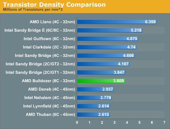
Transistor density depends on more than just process technology. The design of the chip itself including details like the balance between logic, cache and IO transistors can have a major impact on how compact the die ends up being. Higher transistor densities are generally more desirable to a manufacturer (fewer defects per die, more die per wafer, lower costs), but from the end user's perspective the overall price/performance (and power?) ratio is what ultimately matters.


43 Comments
View All Comments
Khato - Friday, December 2, 2011 - link
Do we have any reason to trust the AMD PR department right now? Because what it sounds like to me is that 1.2B may be the functional design transistor count, and 2B may be the actual floorplan transistor count with a nice huge 800M discrepancy because of their lackluster physical design. I mean, those huge 'dead' spaces between the actual logic blocks in the die shot (you can distinctly see each module, L3 cache, and uncore) are almost certainly automated signal routing, and with those kinds of distances it's guaranteed that you're going to have a lot of repeaters...I can easily see AMD PR deciding that it looks bad to be using so many transistors to get such pathetic performance... so why not claim the other transistor number? There's no real way to confirm or deny their number. And they can justify it with the pathetic excuse that they're only using 1.2B transistors on the actual design, even if actual silicon has far, far more.
Phylyp - Friday, December 2, 2011 - link
I now have a question - how do they come up with these numbers? Is it an estimate? Is it a true count at the tape-out point?If its an estimate, I can understand how a changed/improved estimation technique can revise the numbers... though a 40% variation is extremely shoddy.
MS - Friday, December 2, 2011 - link
At 16 MB total L2+L3 cache, the transistor count for those two caches alone comes out as 1.2 B transistorshttp://www.lostcircuits.com/forum/viewtopic.php?f=...
Khato - Friday, December 2, 2011 - link
Indeed. Though the linked post is slightly off as its calculation equates 16M to 16e6 instead of 16*2^20. Using the correct equation results in 1207959552 transistors...So apparently AMD's PR department can count L2+L3 cache transistor numbers?
MS - Friday, December 2, 2011 - link
That's correct but for the proof of the concept I thought I use the simplified decimal metrics instead of the binary equation. Otherwise, who knows what kind of algebraic abuses I would see in the replies.Khato - Friday, December 2, 2011 - link
Haha, fair enough. Either way, the end result is quite amusing.Khato - Friday, December 2, 2011 - link
And now to reply to myself as I wake up a bit more...The number is more likely around 900M for the L2+L3 cache as they appear to be using 6T sram as usual there. Still, the point stands that the 2B transistor number seems about right.
MS - Friday, December 2, 2011 - link
Yes, I updated my post accordingly as well.Chaki Shante - Friday, December 2, 2011 - link
Correct me if I'm wrong, but I thought that transistor count was never an exact figure. Designers usually get a NAND equivalent gate count, from their design tools, as if all gates were the same type so this is a first approximation. Then transistor count is derived by simply multiplying by a factor of 4, the number of transistors in one Nand gate. Can it explain the discrepancy?MS - Friday, December 2, 2011 - link
Yes, it could, at least to a certain degree. Specifically, if AMD applies the "logic transistor" footprint to the overall used die size, i.e. the parts that really have some functional transistors as opposed to some areas that are interspersed as fillers - physical connections (which there are plenty of on BD). This might give you one number for the transistor count.Now, as mentioned in various locations, cache / SRAM transistor footprint is substantially smaller than logic or, to put it differently, the packing is much denser. So if you applied logic transistor density to cache area, you get a pretty wrong number - it will depend, among other things also on the specific SRAM cell and so on.
So yes, in general you are correct and I have a hunch that the 2 B vs. 1.2 B would come out quite well if you just do that type of "Stupid math" without differentiating between die areas. In that case, both numbers would be wrong and the real transistor count would probably be more in the area of 1.75-1.8 B transistors total.
I have left messages with AMD but received not a single word of feedback.