Western Digital Announce BiCS4 3D NAND: 96 Layers, TLC & QLC, Up to 1 Tb per Chip
by Anton Shilov on June 28, 2017 10:00 AM EST
Western Digital on Tuesday formally announced its fourth-generation 3D NAND memory, developed as part of the Western Digital/Toshiba joint venture. The fourth-generation BiCS NAND flash chips from Western Digital feature 96 layers and will include several capacity points and will use TLC and QLC architectures. The company expects to start volume production of BiCS4 chips in 2018.
NAND dies that belong to the fourth-generation BiCS 3D NAND will use 96 word layers to minimize die size of the chips and maximize output of fabs, and at this point represents the largest layer count in the flash memory industry. Furthermore the range of BiCS4 NAND die configurations available will be considerably more diverse than BiCS3, which currently only includes 256 Gb and 512 Gb dies. Western Digital plans to offer BiCS4 components based on TLC (triple level cell) and QLC (quadruple level cell) configurations. with capacities ranging from 256 Gb to 1 Tb.
It is noteworthy that Western Digital’s BiCS4 lineup will include QLC NAND, which has been discussed by Western Digital (and SanDisk before that) for several years, but which is about to become reality only in the coming quarters. To store four bits per cell (with 16 voltage states) Western Digital had to use a “thick” process technology alongside multi-layer 3D NAND to keep the per-bit costs down. The company is not specifying how many program/erase cycles its 3D QLC NAND will handle, but various industry predictions over the years have suggested 100 – 150 P/E cycles as a reasonable goal for QLC NAND, which is considerably lower than approximately 1000 P/E cycles supported by TLC NAND. Given such endurance, it is logical to expect 3D QLC NAND to be used for primarily removable storage as well as for ultra-high capacity datacenter drives for the so-called near-WORM (write once read many) storage applications. For example, Toshiba last year discussed a QLC-based datacenter SSD with 100 TB capacity for WORM apps.
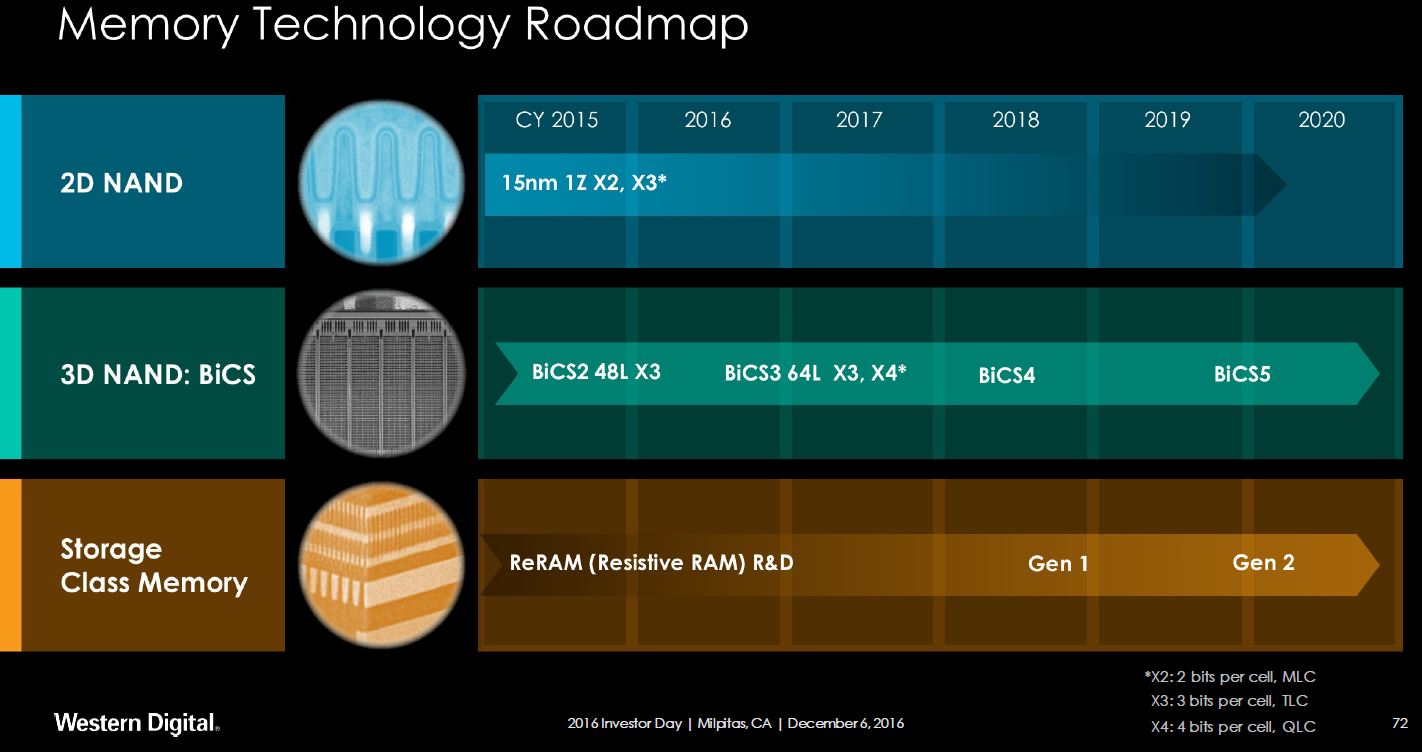
Western Digital plans to begin sampling of select 96-layer BiCS4 3D NAND configurations in the second half of this year, but the manufacturer does not specify which dies will sample when. As for mass production, Western Digital intends to start volume manufacturing of their 96-layer 256 Gb 3D NAND in 2018, with other dies to follow later. Based on Western Digital’s announcements made earlier, the company will gradually introduce more sophisticated BiCS4 96-layer configurations in 2018 and 2019, before moving to BiCS5 sometimes in 2020. That said, it makes sense to expect the highest capacity BiCS4 ICs to ship later rather than sooner.

Finally, Western Digital did not disclose whether it uses NAND string stacking technology to assemble its 96-layer 3D NAND dies, but it is a likely scenario given what industrial publications have been predicting.
Related Reading:
Source: Western Digital


22 Comments
View All Comments
jjj - Wednesday, June 28, 2017 - link
The first is 256Gb, they state that.The Toshiba press release provides some additional insight.
"This 96-layer BiCS FLASH™ will be manufactured at Yokkaichi Operations in Fab 5, the new Fab 2, and Fab 6, which will open in summer 2018. "
So they won't ship much in 2018 if the fabs open in the summer but they might ship a little if nothing goes wrong.
"a capacity increase of approximately 40% per unit chip size over the 64-layer stacking process"
50% more layers, 40% increase in capacity, remains to be seen why and if it's about enabling QCL or 96 layer without string stacking.
You do need to slow it down with the string stacking rhetoric before you have at least some kind of hint that Tosh/WD are using it. The other week you made the claim that their 64L is using string stacking and there is zero support for that claim Today you assume that this product that is 1.5 years away uses it but that's also baseless. They might use it but we got no reason to assume one way or the other.
DanNeely - Wednesday, June 28, 2017 - link
I'm not reading that the way you are. I think the "will open in summer 2018" qualifier is only applied to Fab 6. Fabs 5 and 2's timelines are independent of that fab 6 project.jjj - Wednesday, June 28, 2017 - link
Conversion disrupts output, they are better off ramping the new capacity first and converting the other 2 location once they get to yield.DanNeely - Friday, June 30, 2017 - link
Worn out hardware and older processes disrupt the ability to make money with an old factory. Upgrading them periodically is a mandatory cost of business. And at the level of a large factory the hardware has to be ordered years in advance. You can't decide to delay it for six months or a year if you misjudged the boom/bust cycle unless you've got a factory sized warehouse to stash a factory's worth of new gear or are willing to piss off your suppliers. The latter ends to have bad consequences the next time you go shopping to build/upgrade a factory.Kristian Vättö - Wednesday, June 28, 2017 - link
"50% more layers, 40% increase in capacity, remains to be seen why"Only the memory array is increasing in density. Peripheral circuitry, IO logic, row decoders etc eat up 20-30% of the die area.
jjj - Wednesday, June 28, 2017 - link
Think about that again. You have a X mm2 die with Y array efficiency, you add 50% more layers, if array efficiency remains flat, you gain 50% density. If array efficiency decrease by a bit, it's still far from justifying the gap here.DanNeely - Wednesday, June 28, 2017 - link
AFAIK little or none of the control circuitry around the flash is stacked, as you add more flash cells to the stacks you need more of all the per cells parts which eat into die area.Kristian Vättö - Wednesday, June 28, 2017 - link
You got me there. This is what happens when posting right after work... Anyway, the real reason likely lies in the wordline connectors due to the staircase design. As more layers are added, the die area consumed by the connectors increases.jjj - Thursday, June 29, 2017 - link
That's a fair point but i'm not sure it's that meaningful.The big questions here are QLC and 96 layer. 96 could be sting stacked , i don't think it is as going from 64L to 2x48L can be difficult from a cost perspective. 96L in one is doable but gonna be tricky and they might need thinner films but that's not without issues. Micron will likely stay with string stacking , makes sense for them after 2x32L.
Then there is endurance for QLC, , the market for WORM is limited and costs still not great so they need to get QLC to good enough in consumer.
So i don't quite expect a straight up scaling, just layers added but all else roughly the same.
Anyway, it seems that they would get to over 7Gb/mm2 with a 1Tb QLC die - their 64L 512Gb TLC is at about 3.88Gb/mm2 - and costs bellow 5 cents per GB, hopefully well bellow.
jjj - Thursday, June 29, 2017 - link
An image for Samsung's 32L that gives us an idea about scale for the staircase https://www.3dincites.com/wp-content/uploads/AndyF...Seems they only need about 20um.