GlobalFoundries Adds 12LP Process for Mainstream and Automotive Chips; AMD Planning 12LP CPUs & GPUs
by Anton Shilov on September 21, 2017 7:00 AM EST- Posted in
- Semiconductors
- CPUs
- AMD
- GlobalFoundries
- GPUs
- Zen
- 14LPP
- Vega
- 12nm
- 12LP
GlobalFoundries on Wednesday announced its new 12LP (leading performance) fabrication process. The new manufacturing technology was designed to increase transistor density and improve frequency potential compared to GlobalFoundries’ current-gen 14LPP tech. The company expects the new process to be used by suppliers of various ICs (integrated circuits), including designers of CPUs and GPUs as well as developers of chips for automotive applications and telecommunication solutions. One of the first customers to adopt the 12LP fabrication process will be AMD.
GlobalFoundries’ 12LP manufacturing technology builds upon the company’s 14LPP process that has been used for high-volume manufacturing (HVM) since early 2016. Just like its direct predecessor, the 12LP relies on deep ultraviolet (DUV) lithography with argon fluoride (ArF) excimer lasers operating on a 193 nm wavelength. GlobalFoundries promises that its 12LP provides a 15% higher transistor density and enables a 10% higher frequency potential (at the same power and complexity) compared to “16/14nm FinFET solutions on the market today”. The company does not elaborate which process it used for comparison, but a naturally guess would be its own 14LPP which the company knows well.
| Advertised PPA Improvements of New Process Technologies Data announced by companies during conference calls, press briefings and in press releases |
|||||
| GlobalFoundries | |||||
| 12LP vs 14LPP |
14HP vs 14LPP |
7nm Gen 1 vs 14LPP |
|||
| Power | - | ? | >60% | ||
| Performance | 10% | ? | >40% | ||
| Area Reduction | 15% | ? | >50% | ||
The new 12LP relies on the groundwork set by the 14LPP, but uses 7.5T libraries, which is one of the ways that enables GlobalFoundries to shrink die sizes by increasing transistor density. Since the library contains different elements, IC developers have to “recompile” their designs to take advantage of the process. Meanwhile, since the 12LP and the 14LPP are very similar, for GlobalFoundries’ existing customers migration path to the 12LP is pretty straightforward. As for others, they are more likely to use the upcoming 7 nm anyway given the fact that it is not far away.
| Comparison of 14 nm Branded Process Technologies | |||||||
| GlobalFoundries 12LP |
GlobalFoundries 14HP |
GlobalFoundries 14LPP ? |
TSMC 16FF |
Intel 14nm |
|||
| Fin Pitch | ? | ? | ? | ? | 42 nm | ||
| Gate Pitch | ? | ? | 78 nm | 90 nm | 70 nm | ||
| Min Metal Pitch | ? | ? | 64 nm | 64 nm | 52 nm | ||
| Gate Height | ? | ? | less than 480 nm | 480 nm | 399 nm | ||
| Metal Layers | 13 | 17 | 13 | unknown | unknown | ||
| Design Library | 7.5T | 12T | 9T | 9T | unknown | ||
To a large degree, the 12LP is GlobalFoundries’ response to various manufacturing technologies that build upon the 14/16 offerings and optimize performance and transistor density that have been introduced by various contract makers of semiconductors over the past few quarters. Some of those processes are branded as “12 nm” (e.g., TSMC’s CLN12FFC and CLN12FFC-ULP) and other continuing to carry the “14 nm” monikers (e.g., Samsung’s 14LPC and 14LPU). All three leading foundries — GlobalFoundries, Samsung and TSMC — have been using their 14/16nm-branded technologies for years and have accumulated a lot of knowledge and experience, which is why they could roll out optimized versions of the processes and concentrate on performance and/or transistor density. In addition to this, GlobalFoundries is positioning the 12LP for automotive as well as RF/analogue applications, so there are certain enhancements related to reliability and ability to work in extreme conditions. In particular, GlobalFoundries promises to build a test chip that can work at extreme temperatures from -40°C to +105°C for Automotive Grade 2 qualification in Q4 2017. Keeping in mind lifecycles in the automotive industry, expect the 12LP to stay with GlobalFoundries for many years to come.
A legitimate question about the 12LP in the context of automotive applications is who will be GF’s primary customer(s) for the process. There are a number of players developing various chips for automotive applications these days, but when it comes to designers of SoCs that need to pack a lot of transistors, run them at high frequency and be Automotive Grade 2, the list shrinks rather dramatically.
“The world is in the midst of an unprecedented transition to an era of connected intelligence,” said GF CEO Sanjay Jha. “This new 12LP technology provides the performance and density improvements necessary to help our customers continue innovating at the system level, as they deliver real-time connectivity and edge processing to everything from high-end graphics and automobiles to industrial applications.”
In the meantime, AMD will be one of the first to adopt the tech and judging by comments made by Mark Papermaster (AMD CTO) and Sunjay Jha, the chip developer will use the 12LP to make both CPUs and GPUs using the tech.
“We are pleased to extend our longstanding relationship with GlobalFoundries as a lead customer for their new 12LP technology,” said Mark Papermaster, CTO and senior vice president of technology and engineering, AMD. “Our deep collaboration with GF has helped AMD bring a set of leadership high-performance products to market in 2017 using 14nm FinFET technology. We are excited to work with GF on its new 12LP process technology as a part of our focus on accelerating our product and technology momentum.”
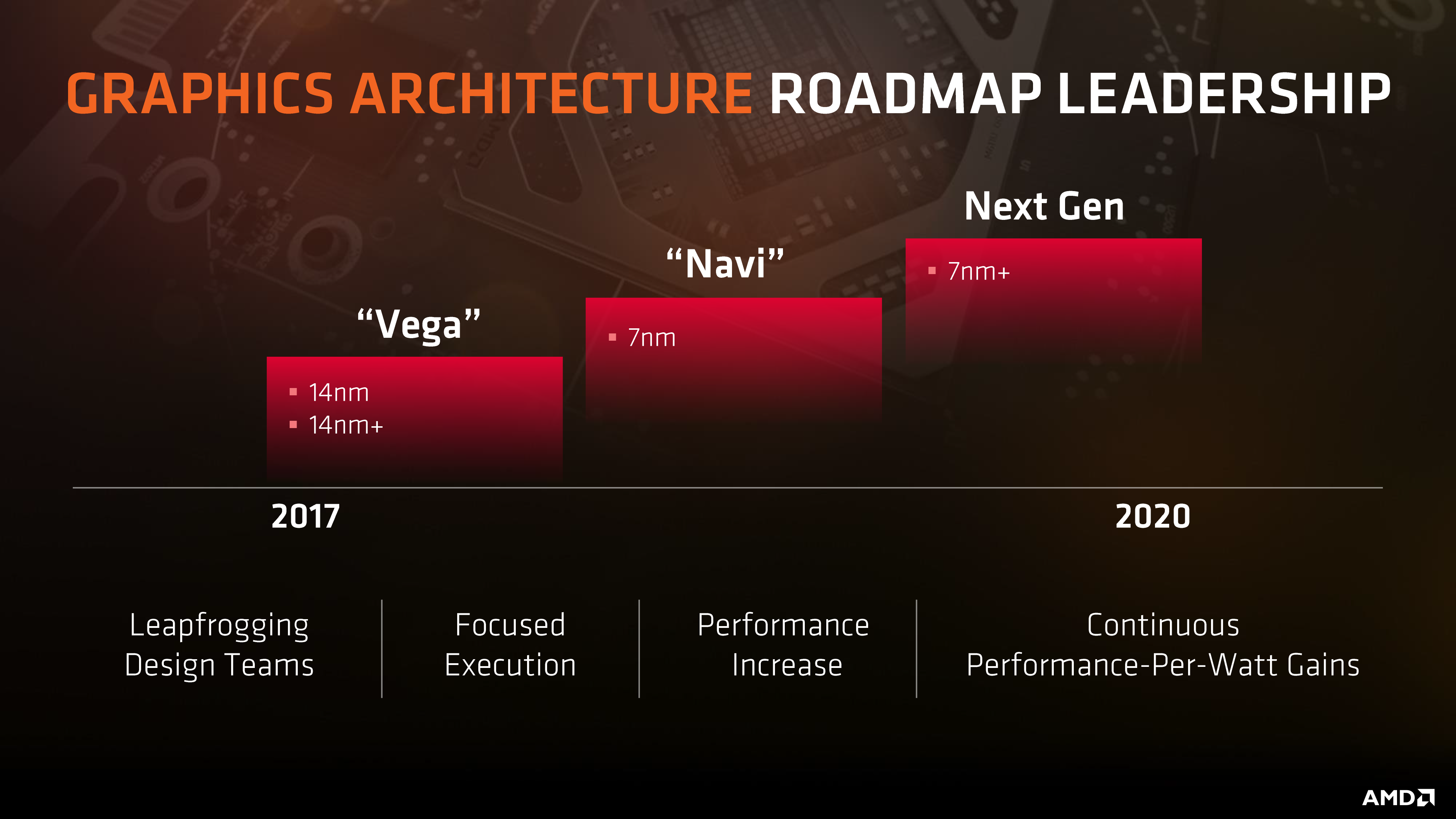
AMD's CPU and GPU roadmaps from earlier this year both listed a "14nm+" node, which at the time was a curious situation since GlobalFoundries didn't have a node between 14nm and 7nm. The obvious takeaway at the time being that GlobalFoundries was developing an interim node - an enhanced version of 14nm - which today's announcement finally confirms. In which case in accordance with Papermaster's official statement, it looks like we should be expecting both Vega and Zen products produced on 12LP in the next year.
To date AMD has said very little about these products. But it's telling that their roadmaps call for existing architectures on the new node rather than their next-generation Navi & Zen 2 architectures, which at least officially, remain scheduled for 7nm. The big question, at least on the GPU side right now, is whether AMD's forthcoming (and still very secretive) Vega 11 GPU is the 12LP product on the company's roadmap, or if AMD is planning on doing a more thorough refresh of Vega at 12LP later on.
Conceptually, all of this is very close to the old "half node" release cadence for GPUs, which would typically see major new GPU architectures released on a new process node, and then smaller and more power-efficient chips released a year later on the interim half node. Half nodes largely died out at 45nm, as fabs opted to put their resources and focus into bringing up whole nodes sooner rather than investing in short-lived half nodes. However as whole node improvements have gone from two year events to three and four year odyssies, it looks like half nodes are back, and with them the refresh chip release strategy.
GlobalFoundries expects to start risk production using the 12LP fabrication technology in Q1 2018. The company does not disclose any timeframes for HVM, but expect them to be different for various chip developers. For example, AMD is a very close partner of GlobalFoundries, so the company gets access to PDKs ahead of many other clients. That said, expect AMD to release its products made using the 12LP rather sooner than later. Mark Papermaster says that the aforementioned chips are to be released in 2018, but he does not elaborate whether to expect them in the first or the second half of the year.
Related Reading:
- Samsung and TSMC Roadmaps: 8 and 6 nm Added, Looking at 22ULP and 12FFC
- GlobalFoundries Details 7 nm Plans: Three Generations, 700 mm², HVM in 2018
- GlobalFoundries to Expand Capacities, Build a Fab in China
- GlobalFoundries Updates Roadmap: 7 nm in 2H 2018, EUV Sooner Than Later?
- AMD Amends GlobalFoundries Wafer Supply Agreement Through 2020, Gaining New Flexibility & New Costs
- EUV Lithography Makes Good Progress, Still Not Ready for Prime Time
Source: GlobalFoundries


32 Comments
View All Comments
MajGenRelativity - Thursday, September 21, 2017 - link
Looks interesting! I hope that 12nm can let AMD push the Zen architecture further to counter any of Intel's potential gains with Coffee LakeSunnyNW - Thursday, September 21, 2017 - link
Agreed, AMD desperately needs clock improvements. With Intel having both an IPC and clock advantage it is going to be interesting to see how much AMD can gain in either stat. Curious to see how the "10%" higher performance of 12LP translates into real world clock speeds for AMD.MajGenRelativity - Thursday, September 21, 2017 - link
If AMD can manage to improve the clockspeed by 10%, I think AMD can remain competitive until the Zen2 architecture and 7nm. I'm not expecting much out of Coffee Lake other than more cores, which is where Ryzen already has things covered.The_Countess - Thursday, September 21, 2017 - link
The 10% is increased performance at the same power level.but really that's already fine with ryzen. significantly better then intel per core even.
The real problem is the clockspeed wall ryzen hits around 4ghz. i HOPE this means that that is also increased, and some improvement seems likely, but we can't really tell from the information given in the article.
MajGenRelativity - Thursday, September 21, 2017 - link
That's what I was thinking too. Have to wait and see.Alexvrb - Thursday, September 21, 2017 - link
The 10% performance uplift they're talking about in this article is strictly from clockspeed gains."GlobalFoundries promises that its 12LP provides a 15% higher transistor density and enables a 10% higher frequency potential (at the same power and complexity)"
So at this point it's really impossible to know what final gains will be, without knowing how much AMD has managed to overhaul Zen in the short time. They've had their hands full with lots of projects. Maybe they've tweaked the design enough to net another 5-10% IPC? Who knows. That, coupled with the frequency increases, would help tide things over.
Personally I'm more interested in whether they can manage to improve CCX-to-CCX latency, and/or boost their IMC's capabilities (which would likewise improve said fabric latency).
0ldman79 - Saturday, September 30, 2017 - link
Just a hunch, but it's probably an architectural problem that has them hung at 4GHz. Stuff like that has happened in the past, pretty sure the FX had a similar issue in it's original release.I'm sure the limitation has been found and if it isn't fixed in the Zen v2 then it will probably be corrected in the third release.
It would be tremendous if they could find as much improvement on Zen v2 as they did on Bulldozer v2.
SunnyNW - Thursday, September 21, 2017 - link
I guess it is true that it will be a while before we see 7nm chips from AMD. AMD only has, so far, ONE cpu chip on 14nm. With the cost of designing a chip sky rocketing I'm sure AMD is not in a hurry to rush out 7nm chips which is something that Papermaster himself has said. Most in the public expect AMD to have 7nm chips by as early as late 2018 but I would guess late 2019 is more realistic.MajGenRelativity - Thursday, September 21, 2017 - link
I was always thinking 7nm was 2019, unless I was mistaken. The AMD slides seemed to suggest late 2018 at the earliest for 7nm. Raven Ridge is another CPU chip on 14nm, and it's bouncing around development and close to release. It's Zen, yes, but still a different die.SunnyNW - Thursday, September 21, 2017 - link
I would not be suprised at all if 7nm was 2020 for AMD and I can see them skipping the initial 7nm for the EUV version to try and save some more money (Yes I know what they have shown in slides regarding their use of 7nm and 7nm+). I personally hope they get even more aggressive with their timelines and push for an accelerated roadmap. Of course this would require more expense but I think it would be worth it for the financial returns.