Phison at CES 2018: Thunderbolt SSDs, Second-Gen NVMe Controllers
by Billy Tallis on January 10, 2018 8:25 PM ESTLAS VEGAS, NV — At CES, SSD controller vendor Phison is showing off a range of controller ICs and drive reference designs that are close to hitting the shelves.
Phison's second generation of NVMe SSD controllers has been on the roadmap for quite a while, but now the products are starting to become a reality. The PS5008-E8 and its DRAMless -E8T variant are Phison's solution for the emerging low-end NVMe product segment. These controllers will be used with 3D TLC NAND flash memory, and their performance will be limited by the use of a PCIe 3 x2 interface instead of the x4 interface used by high-end NVMe drives. The DRAMless E8T controller supports the NVMe 1.3 Host Memory Buffer (HMB) feature to offset the random I/O performance hit that DRAMless SATA SSDs suffer from. The E8 series is in mass production using UMC's 40nm fabrication process. MyDigitalSSD has already started shipping their SBX SSD using the E8 controller, and many other brands will soon be shipping products using the E8 or E8T.
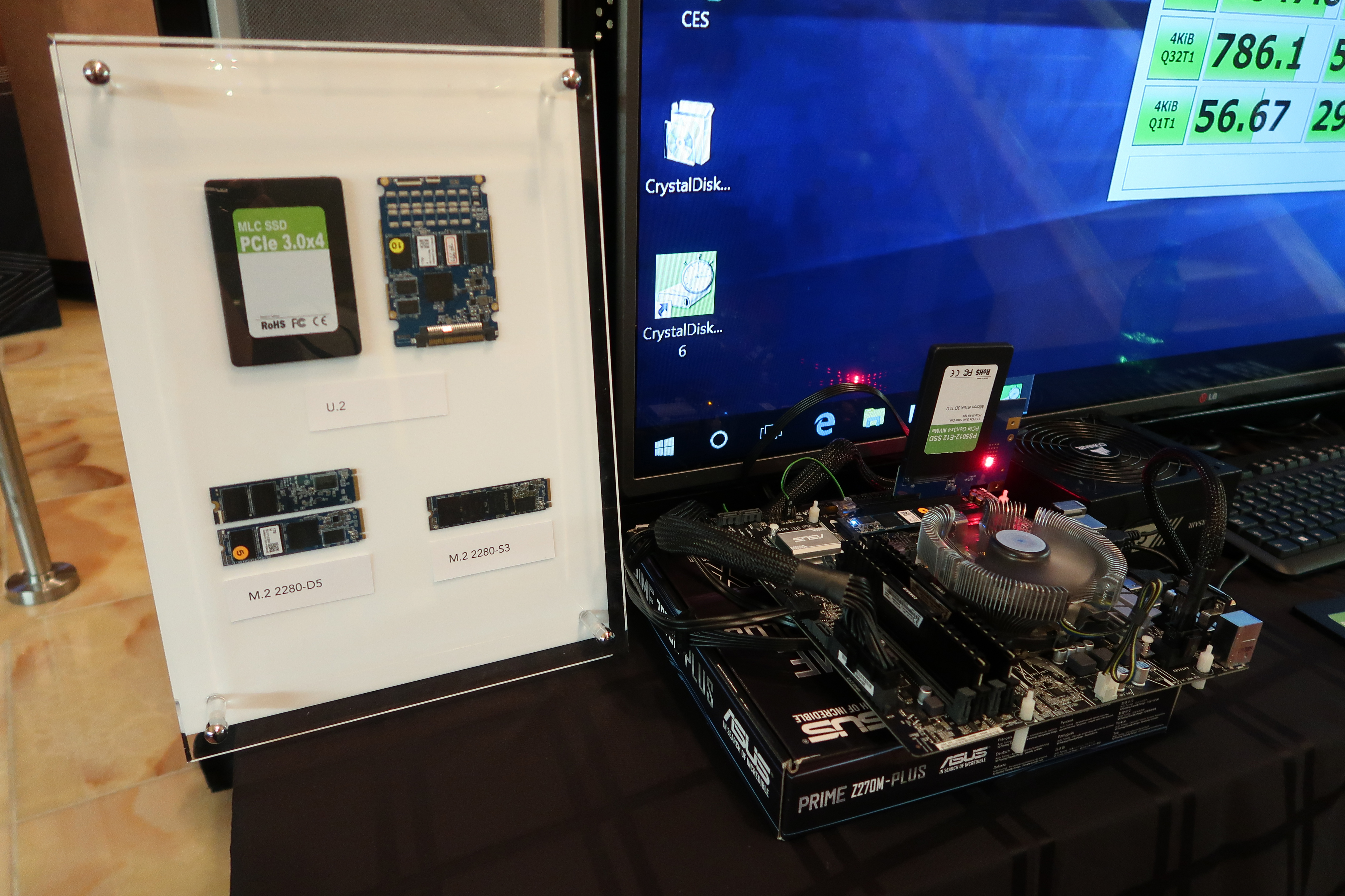
Phison's PS5012-E12 controller is their high-end replacement for the current E7 controller, and it promises to bring much higher performance: over 3GB/s sequential transfers when paired with 64L 3D TLC NAND. Random reads and writes can hit 600k IOPS at high queue depths. It looks like this time around Phison will be much more competitive at the high end as NVMe SSDs start closing in on the limits of a PCIe 3 x4 link.
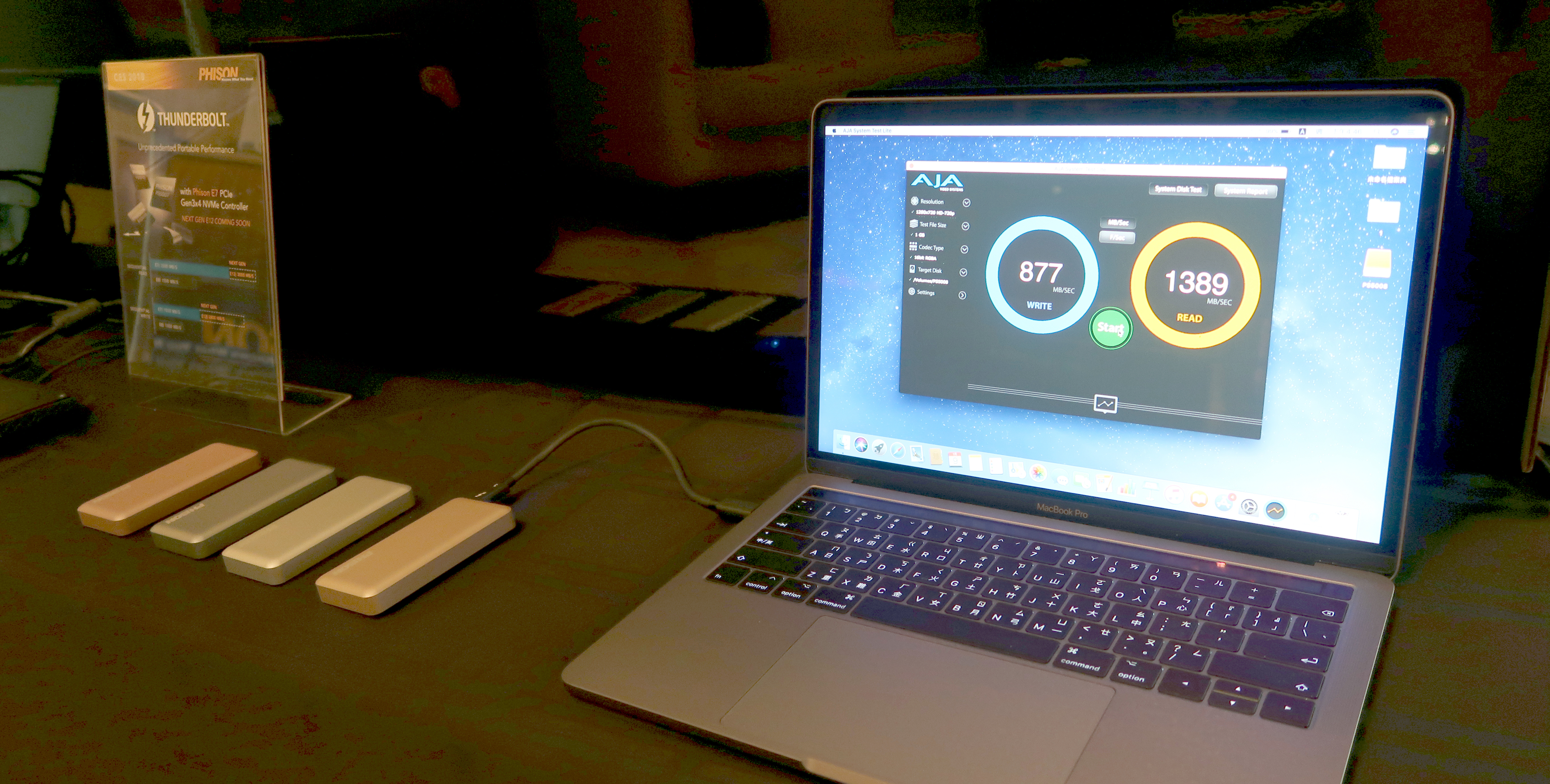
Phison is also showcasing their reference designs for portable Thunderbolt 3 NVMe SSDs. Portable SSDs are high-performance alternatives to USB thumb drives, and typically incorporate a SATA SSD controller behind a USB to SATA bridge. This is more expensive than a single-chip USB flash controller, but puts them in an entirely different league for performance and capacity. Most SATA-based portable SSDs internally use a mSATA or M.2 SATA module. A few products even use two SATA controllers in a RAID0 configuration to offer higher performance: we've tested the SanDisk Extreme 900 and Netac Z5. Phison's Thunderbolt 3 SSDs will blow past all of them. Since these drives simply put a Thunderbolt 3 controller and a M.2 NVMe SSD in a portable housing, it's trivial for vendors to create products based on any of Phison's three NVMe controller options, but the most common configuration to hit the shelves will be with the cheapest E8 controller. Patriot is already showcasing their version of this design.
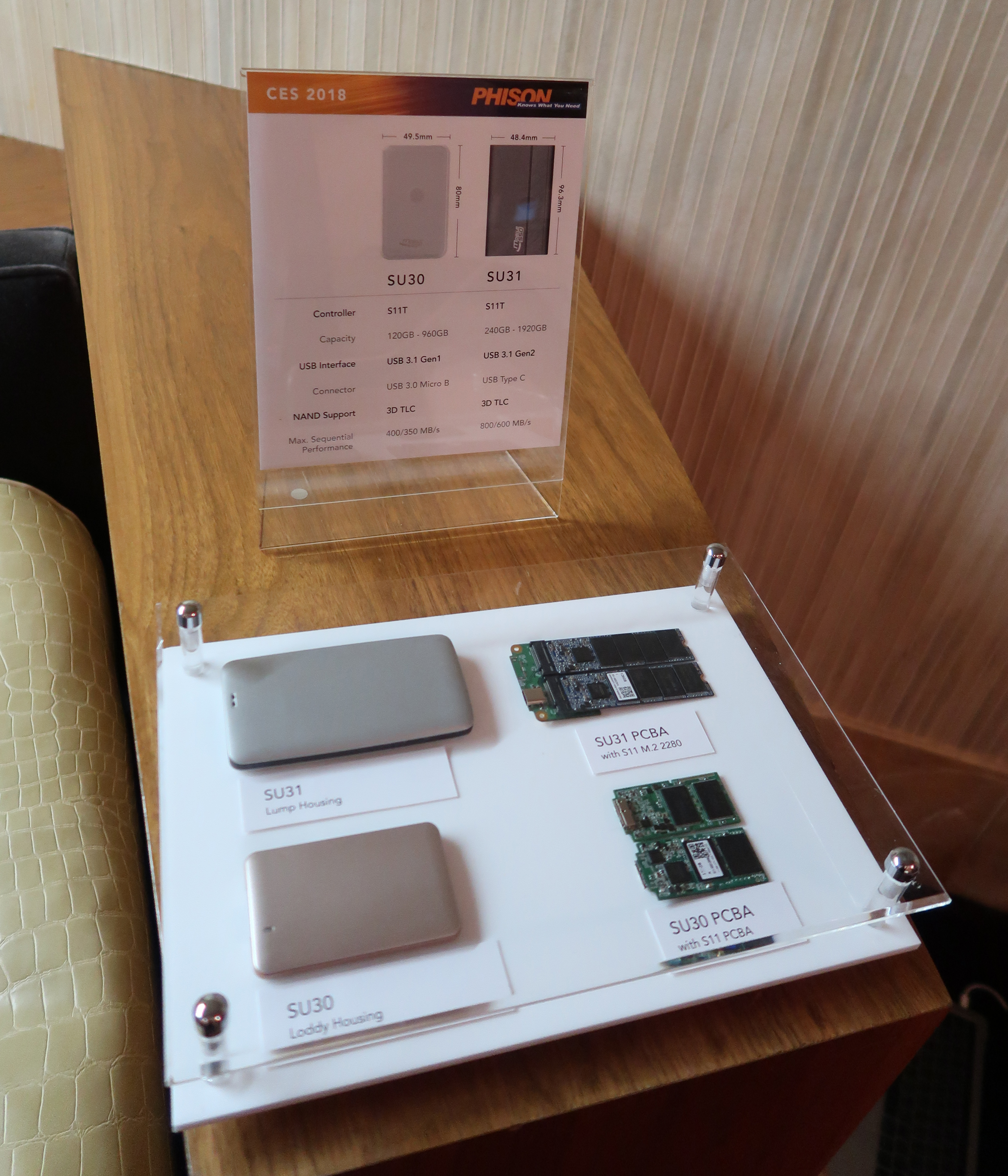
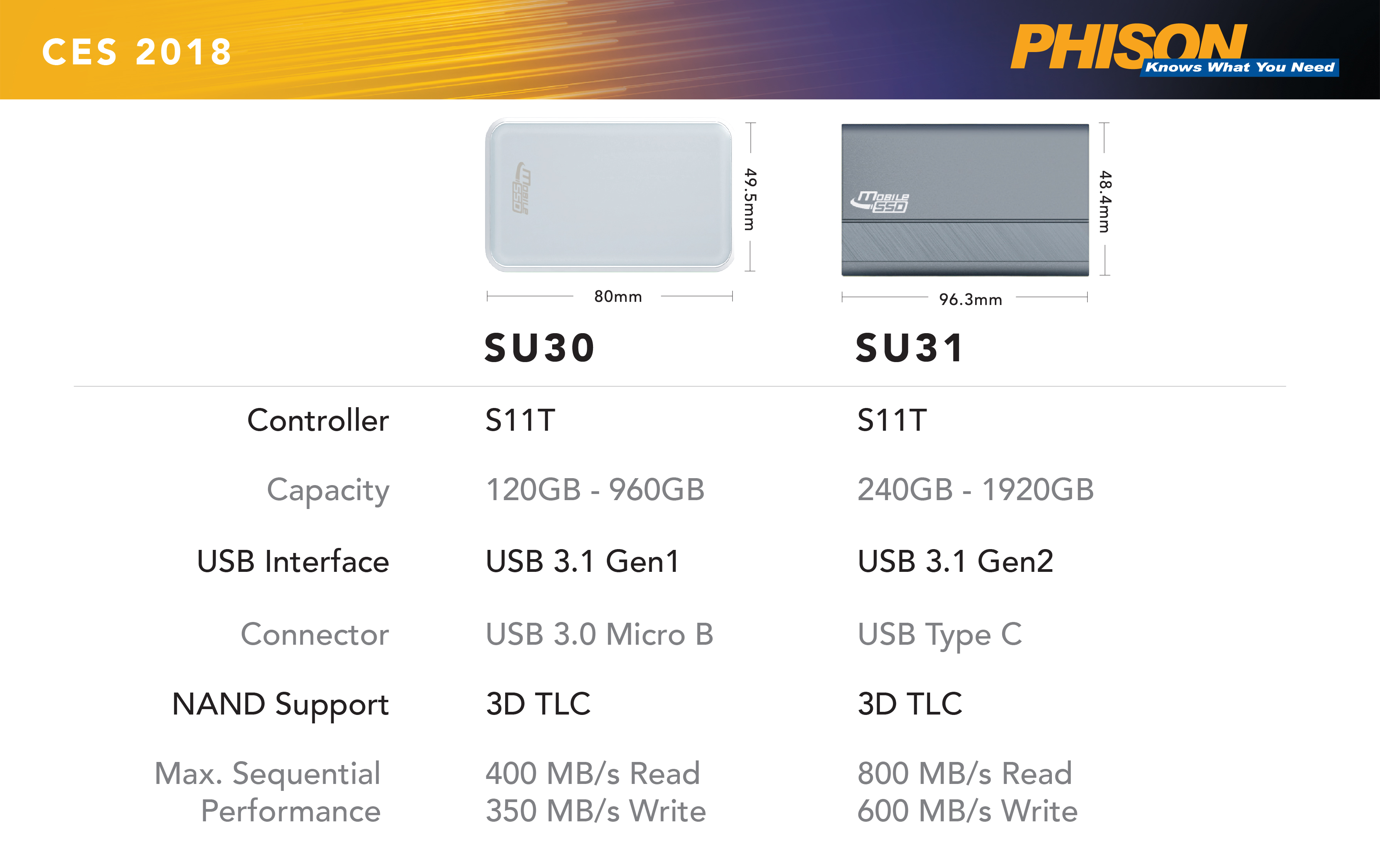
In addition to the Thunderbolt 3 SSDs, Phison is also showing SATA-based Portable SSD designs using one or two of their DRAMless S11 controllers, which was their first controller to support 3D TLC NAND.
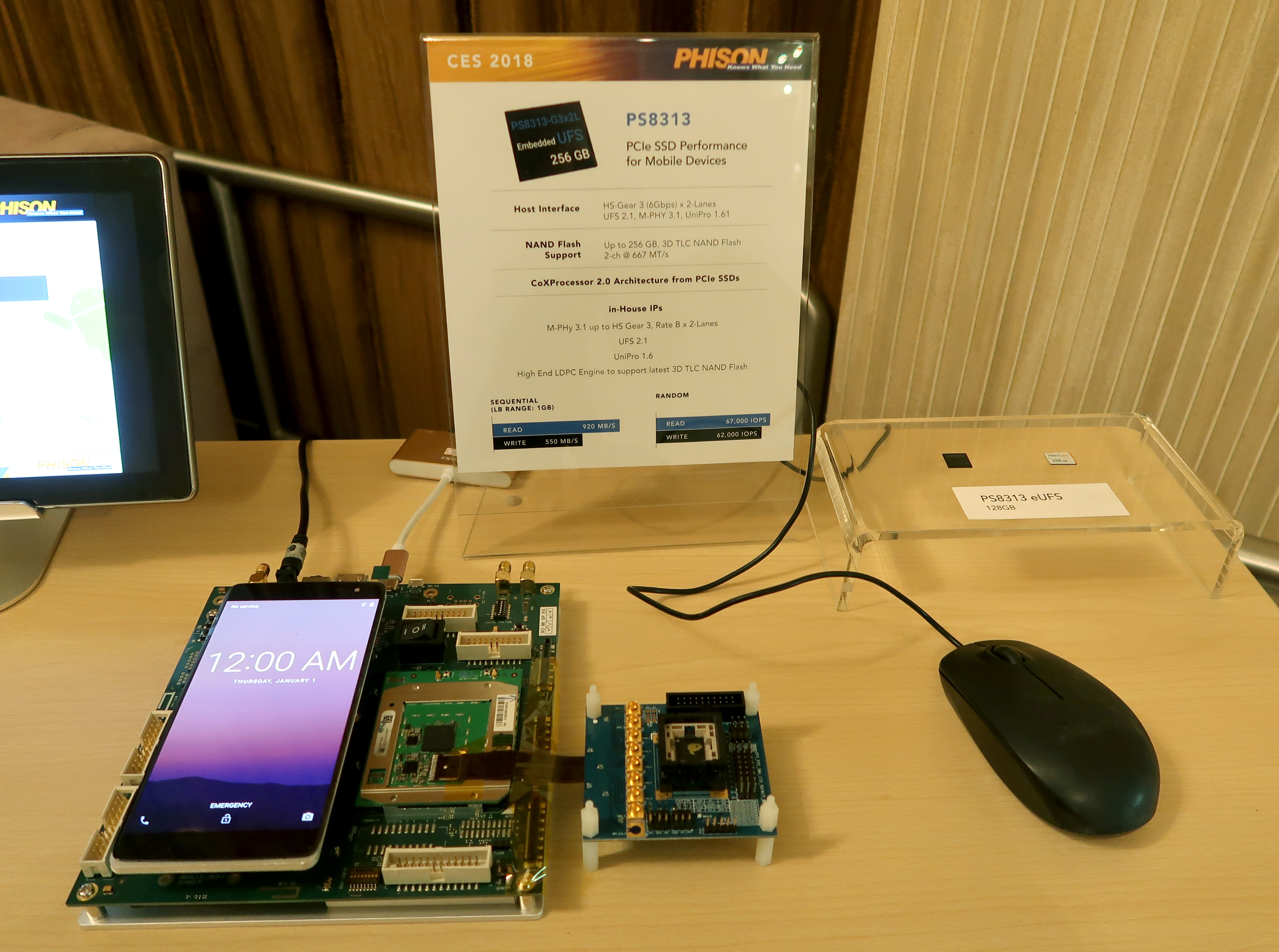
For the mobile market, Phison is also demonstrating their embedded UFS solution for high-performance storage in smartphones and tablets. The new PS8313 controller supports twice the capacity of their current PS8311 thanks to the addition of a second flash interface channel, and substantially higher performance with a two lane host interface.
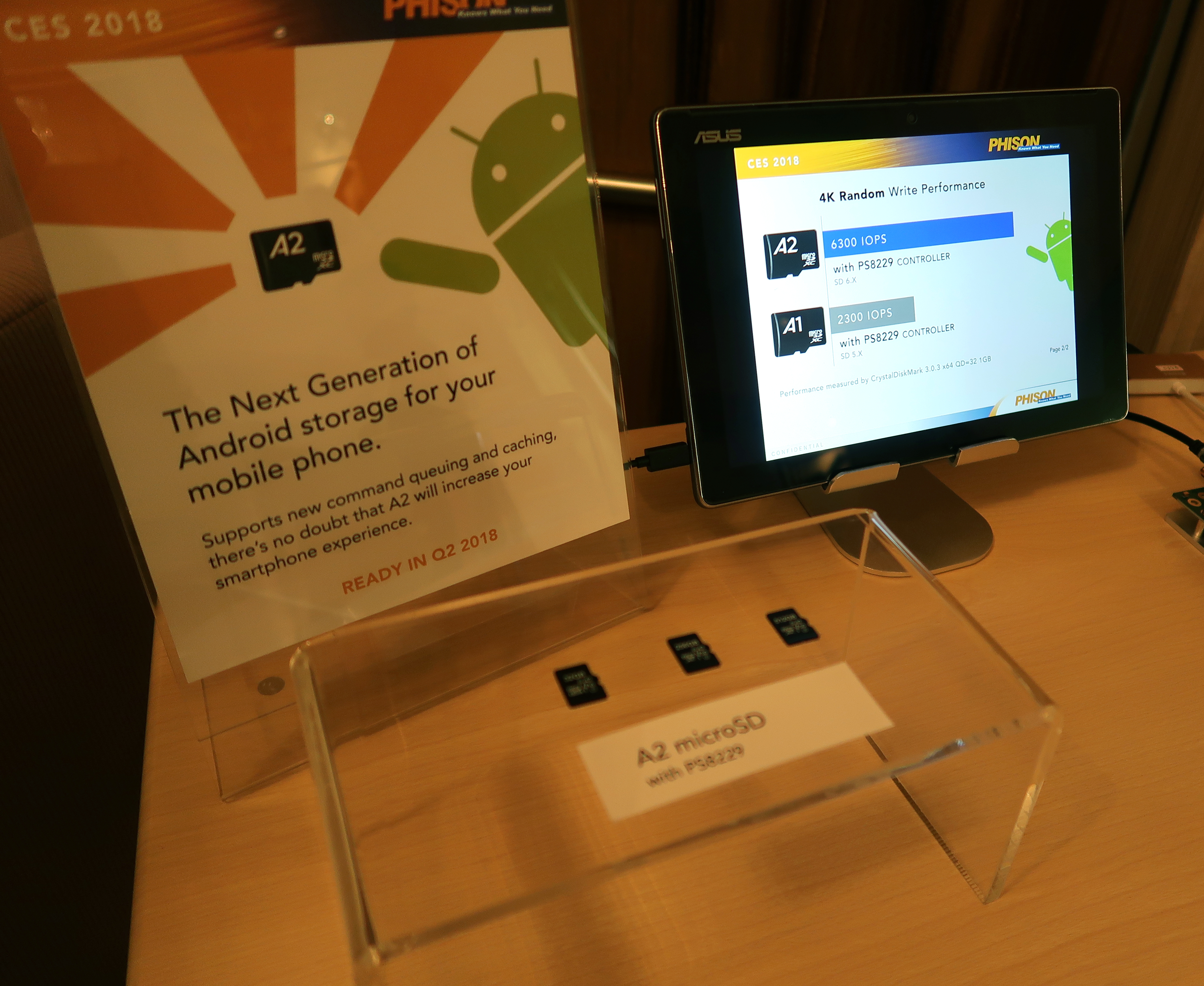
The upcoming PS8229 SD card controller will support the new features of the SD 6.0 standard and meet the requirements for the A2 application performance class when used with a SD 6.0 capable host. This controller is expected to be ready in Q2.


9 Comments
View All Comments
danwat1234 - Thursday, January 11, 2018 - link
Whatever happened to SandForce 3 SSDs?iwod - Thursday, January 11, 2018 - link
That is quite a good question. But My guess is that the market has moved on. In the early days SSD performance varies a lot, may be it still does, but the bottom end of the spectrum is no longer horrible. While the top end is dominated by Samsung which research and develop the controller and NAND as well as assembling the whole SSD. Which there is only space for another side of market chasing cost.Anyway SSD controller no longer brings any new and exiting features other then new IO. ( NVM or PCI-E 4.0 ) We have got Seq Read write, Random Read Write, latency, 99th percentile pause, all under very good control.
I am pretty sure the bottleneck has moved to somewhere else.
AnTech - Thursday, January 11, 2018 - link
What are the makes/vendor of the extermal portable Thunderbolt & USB SSD shown on pictures 2 & 3, respectively, above? Thanks.Dahak - Thursday, January 11, 2018 - link
Think those are just the reference designs by Phison that other vendors can use. The link just above image #3 shows that Patriot has one that looks like the top drive in the Phison picFunBunny2 - Thursday, January 11, 2018 - link
technical question: the piece says it's built on a 40nm process. I've always wondered how TLC on such larger nodes will be supported going forward. the original machinery at such nodes is likely a decade or more old. so: 1) are the equipment manufacturers still in the business of making/supporting such machines and 2) it's obvious that a 40nm machine can't make 20nm parts, what about the other way round? is the XXnm spec hardwired throughout the process, or can any node size down to XX be simply dialed in? if the latter, then capacity is fungible essentially forever. if not, will the NAND business be like the car business in Cuba?Billy Tallis - Thursday, January 11, 2018 - link
It's one of Phison's SSD controllers that is made on a 40nm process. That controller can manage current generation NAND flash.There are quite a few silicon foundries that are running older process nodes. They're very cost effective for chips that don't need super high transistor counts or high performance. Phison's E8 would probably be more power efficient if it was built on a 28nm process like the E12 is, but it wouldn't be any faster and it would be more expensive. Likewise, moving something like the E12 to a 14nm FinFET process would be expensive and offer little benefit.
dusty5683 - Thursday, January 11, 2018 - link
Good question, and to preface this I'm definitely no semi-process guy. To be clear the 40nm is referring to the process capability that the controller was built on not the actual NAND. These numbers are "usually" minimum feature sizes, many parts of the controller will be built with feature sizes much bigger than 40nm. In SOC's, NAND and DRAM many of the interconnect pathways are much larger, 60nm and above still. Tools are not designed to produce a specific process size. They are built to be capable of certain resolutions and manufacturers use all sorts of different tricks to get the minimum process shown here, such as pitch doubling or nowadays pitch quadrupling. So, some of these tools may not be brand new, but don't think of them as outdated. Larger feature sizes on some parts of the chip are still very useful.fFunBunny2 - Thursday, January 11, 2018 - link
"To be clear the 40nm is referring to the process capability that the controller was built on not the actual NAND."I got that part, but the mention of 40nm as process reminded me that TLC is said to be built on nodes about that same size/age. which lead to the question.
kn00tcn - Friday, January 12, 2018 - link
logically i would expect high resolution machinery to be able to work with lower resolutions, it's simply distance between metal walls/objectsit's not like a chip is a bed of nails, some tunnel connection between two areas for example could be considered 200nm length by 14nm width (probably)