TSMC Details 5 nm Process Tech: Aggressive Scaling, But Thin Power and Performance Gains
by Anton Shilov on May 8, 2018 4:20 PM EST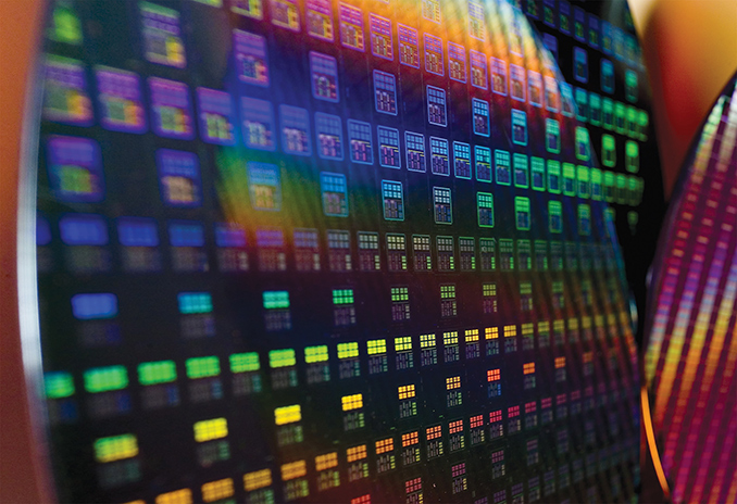
At a special event last week, TSMC announced the first details about its 5 nm manufacturing technology that it plans to use sometime in 2020. CLN5 will be the company’s second fabrication process to use extreme ultraviolet (EUV) lithography, which is going to enable TSMC to aggressively increase its transistor density versus prior generations. However, when it comes to performance and power improvements, the gains do not look very significant.
Just like other fabs, TSMC will gradually ramp up usage of ASML’s Twinscan NXE:3400 EUV step and scan systems. Next year TSMC will start using EUV tools to pattern non-critical layers of chips made using its second-gen 7 nm fabrication technology (CLN7FF+). Usage of EUV for non-critical layers will bring a number of benefits to the CLN7FF+ vs. the original CLN7FF process, but the advantages will be limited: TSMC expects the CLN7FF+ to offer a 20% higher transistor density and a 10% lower power consumption at the same complexity and frequency when compared to the CLN7FF. TSMC’s 5 nm (CLN5) technology will increase the usage of EUV tools and this will bring rather massive advantages when it comes to transistor density: TSMC is touting a 1.8x higher transistor density (~45% area reduction) when compared to the original CLN7FF, but it will only enable a 15% frequency gain (at the same complexity and power) or a 20% power reduction (at the same frequency and complexity). With the CLN5, TSMC will also offer an Extremely Low Threshold Voltage (ELTV) option that will enable its clients to increase frequencies of their chips by 25%, but the manufacturer has yet to describe the tech in greater detail.
The rather small, incremental improvements that TSMC is discussing for the CLN7FF to CLN7FF+ and CLN7FF+ to CLN5 transitions indicate that it gets increasingly harder to offer decent gains from generation to the next. It remains to be seen whether all of TSMC’s leading-edge customers will keep adopting all the latest process technologies that the company offers, or will miss certain cycles given small incremental increases, but large companies (such as Apple) adopted all the latest fabrication processes in the recent years (i.e., it made economic sense to adopt them).
| Advertised PPA Improvements of New Process Technologies Data announced by companies during conference calls, press briefings and in press releases |
||||||||
| TSMC | ||||||||
| 16FF+ vs 20SOC |
10FF vs 16FF+ |
7FF vs 16FF+ |
7FF vs 10FF |
7FF+ vs 7FF |
5FF vs 7FF |
|||
| Power | 60% | 40% | 60% | <40% | 10% | 20% | ||
| Performance | 40% | 20% | 30% | ? | higher | 15% | ||
| Area Reduction | none | >50% | 70% | >37% | ~17% | 45% | ||
Moving on to the readiness of TSMC’s process technologies with EUV, “Foundation” IP for CLN7FF+ has been validated in silicon, but various important blocks required for 28–112G SERDES, embedded FPGAs, HBM2, and DDR5 interfaces will not be ready before late 2018 or even early 2019. Fully certified EDA flows for CLN7FF+ will be ready by August. Meanwhile, EDA flows for CLN5 are in their infancy: version 0.5 will be ready by July and numerous IP blocks (PCIe 4.0, DDR4, USB 3.1, etc.) will not be ready until 2019.
Next up is equipment readiness. As reported, TSMC is building a separate fab to make chips using its CLN5 process technology. The new Fab 8 will use numerous Twinscan NXE:3400 scanners, but TSMC admits that at present the average daily power levels of the light sources for their EUV tools is only at 145 W, not enough for commercial usage. Some of the tools can sustain 250 W production for a couple of weeks and TSMC has plans to hit 300 W later this year, but EUV tools still need improvements. There are also some issues to be solved with things like pellicles (they transmit 83% of EUV light and are expected to hit 90% next year), so EUV lithography in general is not ready for prime time just now, but is on track for 2019 – 2020.
Related Reading:
Source: EETimes


10 Comments
View All Comments
ZolaIII - Tuesday, May 8, 2018 - link
You could had at least change a title from EETimes. You know there's people hire who do read D&R. This will even be funny to Realjjj.prisonerX - Tuesday, May 8, 2018 - link
In this day and age, 15 or 20 percent frequency and power scaling seems perfectly decent to me. We're at the end of the road, folks, and are getting diminishing returns on this one simple trick to improve performance. It's over.Nearly 2x area scaling though seems like great news. More space for more cores and more parallel workloads sounds good to me.
CiccioB - Wednesday, May 9, 2018 - link
You have to consider that there are two problems with these limitations (no frequency scaling and decrease of power usage):1. the more transistor you put in the die more heat power you have to dissipate, and the smaller the surface the higher its density which is problem n.1 for power dissipation. THere would b no problem dissipating 1000W if the die surface were 10cm^2. But we are in mm^2 constrained domain, so putting more transistor all running at high frequency is an added problem
2. performance scaling is related to frequency scaling (or IPC) not to the number of core you have available. There's only a tiny number of algorithms and applied works that scale indefinitely with the number of available cores. Most of the algorithms can't be threaded, the few that can needs a lot of work (programming wise) and add overhead, so they do not scale linearly and having 64 cores at 1GHz do not help them going faster than a dual core at 4GHz,
GPUs may be the devices that can nonetheless benefit from this transistor shrinking especially if they can limit power usage (AMD has to work a lot on this side).
However these limitations make MCM configurations more appropriate. They have all the characteristics for continuing lowering the price while being able to dissipate more power provided the communication channels are powerful enough (in terms of bandwidth and latency).
MCM-GPU most critical problem is bandwidth with NUMA configuration. We already see the problem with a CPU like ThreadRipper that uses about 1/10 of the bandwidth of a GPU.
peevee - Tuesday, May 8, 2018 - link
Don't forget that it is their best estimates before reality kicks in.Dragonstongue - Tuesday, May 8, 2018 - link
or is an educated guesstimate ^.^I suppose it could go either way, likely if they know it will be even better than this they are likely not to pre warn other fabs (such as Intel) so whatever secret sauce that they can pull at the last minute will allow them to have that small advantage against others (maybe not Intel but GF/Samsung for sure if anyone)
Time will tell as it always does.
I suppose as other person above said, if scaling is where should be, even if there is not an awesome clock speed improvement or whatever, it could allow more cores etc to "make up the difference" and the way things are going, it will be how many cores can they stuff per "chip" that will rule the day going forward.
they can only get so many transistors per mm2 and can only get them running so fast when doing SOI/FD-SOI/FinFet or whatever (limitation of silicon and power/temperature constraints) so instead of chasing crazy quick clock speeds they can instead engineer it to get as many small features as possible to dedicate some of the "speed" for instead "more cores" to stick within the design rules
something along those lines anyways.
MobiusPizza - Tuesday, May 8, 2018 - link
Why is there performance scaling number for 10FF vs 16FF+ and 7FF vs 16FF+ but 7FF vs 10FF is marked with a question mark? Surely you can calculate that to be below 10%, as 16FF+ to 10FF gives 20% while 16FF+ to 7FF gives 30%.smilingcrow - Wednesday, May 9, 2018 - link
5FF appears to be about 5 times denser than 16FF+ which is great for adding more cores. But as someone else pointed out the power density will be an issue for desktop/server although maybe not for mobile.Opencg - Thursday, May 10, 2018 - link
If we continue at this rate we will be at .1nm by 2030 AND we will have a self sustaining mars base thanks to elon musk.benzosaurus - Sunday, May 13, 2018 - link
Or at least we would be, if 0.1nm weren't about the diameter of hydrogen atom, and individual hydrogen atoms make pretty lousy insulators and semiconductors.0ldman79 - Friday, October 5, 2018 - link
Yep. We're getting to the end of the current growth of lithography.They're going to have to approach the problem differently very soon.