Intel Provides Royalty-Free License for Data Bus to DARPA’s Modular Chips Initiative
by Anton Shilov on July 25, 2018 2:00 PM EST- Posted in
- Semiconductors
- Intel
- EMIB
- DARPA
Taking place this week is DARPA’s 2018 Electronic Resurgence Initiative (ERI) Summit, the defense research agency's first gathering to address the direction of US technology manufacturing as Moore's Law slows down, and how the agency can jumpstart alternative efforts to ensure continued performance scaling. To that end, in an interesting and unexpected move from the summit, Intel has announced that it would offer a royalty-free license for its Advanced Interface Bus (AIB) to participants of the agency’s Common Heterogeneous Integration and Intellectual Property (IP) Reuse Strategies (CHIPS) program. The move will help interested parties to design SoCs utilising heterogeneous components made using different process technologies.
Modern, complex chips are hard to manufacture and equally hard to design, as they frequently contain a number of different application-specific functional blocks (e.g., general-purpose cores, graphics cores, etc.). In a bid to somehow reduce costs of chip design, numerous companies have come up with modular development approaches that allow them to design SoCs using more or less standard components. This methodology is used to develop modern SoCs for mobiles, game consoles, and other consumer electronics. However, it is largely believed that the approach is still not enough cost-effective for future SoCs, as the entire chip must still be manufactured as a single, monolithic die. As a result, Intel has propose using so-called chiplets, which are heterogeneous components of a chip produced using different process technologies and interconnected using its AIB interface.

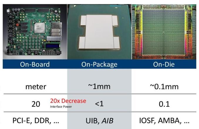
Intel’s Advanced Interface Bus is a low-power die-to-die interface that is based on a forward clock parallel I/O architecture. AIB features a 1 Gbps per lane SDR transfer rate for control signals and a 2 Gbps per lane DDR transer for data. AIB is agnostic to particular packaging technology used: it can rely on Intel’s own EMIB, or can use other packaging technologies (e.g., CoWoS, InFO, etc.) too. Intel itself of course uses its AIB for its Stratix 10 FPGAs (more on this here), but since the tech is universal, participants of the CHIPS program will be able to use the interface for whatever projects they are working on.
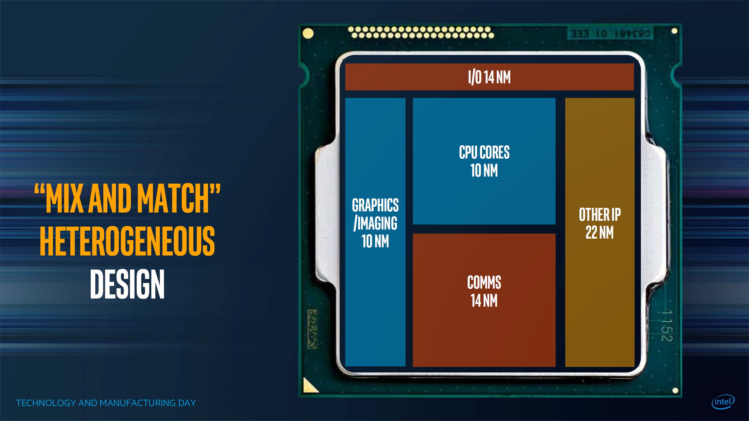
The whole idea behind the CHIPS initiative is to enable developers of SoCs to re-use existing semiconductor blocks for future projects, and to only build blocks on the smallest/most powerful (read: expensive) manufacturing process that part requires. Intel itself proposes to use 10-nm CPU and GPU cores along with communication blocks produced using a 14 nm fabrication process, as well as other components made using a 22 nm manufacturing tech. For developers who do not have access for Intel’s technologies and who have considerably lower R&D budgets, it will make sense to re-use some of the IP produced using a planar fabrication process with processing cores made using a leading-edge FinFET technology.
It remains to be seen when participants of DARPA’s CHIPS program actually start to use Intel’s AIB, but the fact that they now have a technology that could wed leading-edge IP with proven blocks looks rather promising.
Related Reading:
Source: Fuse.Wikichip.Org


14 Comments
View All Comments
Morawka - Wednesday, July 25, 2018 - link
This is what i've been dreaming of for years. Makers and inventors will be pleased.I always wondered if DARPA was secretly working with Intel. With DARPA's nano robotics designs and Intel's lithography, the possibilities become endless.
austinsguitar - Wednesday, July 25, 2018 - link
i give this a solid 20 years until actually realized. nothing to see here. move along.smilingcrow - Wednesday, July 25, 2018 - link
Stevie Ray is disappoint.skavi - Wednesday, July 25, 2018 - link
Ryzen is already using multiple die.Dragonstongue - Thursday, July 26, 2018 - link
^ this..AMD with IF, their APU designs and IMHO "leadership" when it comes to multi-die design "is better" are they "as fast" per core, no, but when they figure out the "secret sauce" of reducing latency, figuring out uncore (voltage/power/heat reduction) and making XFR even more "robust" Intel will be in a "world of hurt"GPU have been built like this for many years in their own fashion...I think the "stacked die" is that much more impressive, if they can figure out how to keep multiple high performance dies cool under pressure, the upcoming chips 2/5d-3d "stacked" are going to be sick.
cannot wait to see the integrated liquid cooling "in the core" something IBM was working on for many years and a good chunk of their design team is "helping" AMD going forward.
will be very interesting over the next couple of years ^.^
edzieba - Thursday, July 26, 2018 - link
Kind of. Infinity Fabric over PCB makes a Ryzen/Threadripper 'chip' effectively a multi-CPU board stuffed into a tiny package, with all the NUMA issues that entails. The idea of Modular Chips is to be able to assemble the (already logically discrete) components into a single chip that, for all intents and purposes, performs identically to a monolithic die.Samus - Thursday, July 26, 2018 - link
They aren't completely "modular" though. You can't just pull one out and have it continue working. You can't even really disable one without screwing up the infinity fabric.There is nothing even remotely close to production in what is being described here.
Alexvrb - Thursday, July 26, 2018 - link
Well... AMD can disable them. First gen TR had two disabled dies.rahvin - Wednesday, July 25, 2018 - link
I give it infinity. Just like the modular cell phone it will be too complicated, too expensive and just plain not worth it once they try to engineer it. Like most ideas it will die during the engineering phase where they actually try to make it work.Dragonstongue - Thursday, July 26, 2018 - link
HBM memory is basically EXACTLY this, as is Ryzen in many ways, much more "modular" then all previous processors AMD has ever made, APU "ties" the concept of cpu and gpu together, HBM "interposer" ties the memory a step further and infinity fabric is the "backbone"so basically AMD has been doing this for what ~7 years or something like that, little chunks at a time refined and "perfected" in their own manner.
small blocks that perform well are much easier to "tie together" than a massive die, glue or not, do it right and latency means very little "at the end of the work load"
if anything, the higher the memory i.e DDR4, DDR5 etc which has increasingly high latency BUT higher bandwidth will vastly benefit the concept compared to trying to do this many years ago with very low latency but slow memory.
interesting if you "spin" the thought in different ways...I think Intel is likely to cheap out and use thermal paste AH HA HA