Hot Chips 2018: IBM Power9 Scale Up CPU Live Blog
by Dr. Ian Cutress on August 21, 2018 7:55 PM EST- Posted in
- CPUs
- Hot Chips
- Trade Shows
- Enterprise CPUs
- IBM
- OpenPOWER
- Live Blog
- POWER9
07:58PM EDT - The biggest part of the show are the server talks in the last session of the last day. All four talks are worth covering, and the first talk is from IBM, detailing both its newest Power9 'Scale Up' version of its processor family, as well as an introduction to PowerAXON, its new connectivity IP. The talk is set to start at 5pm PT / midnight UTC.
08:02PM EDT - Talking about Power9 and the future
08:02PM EDT - Each Power generation is a 'family'
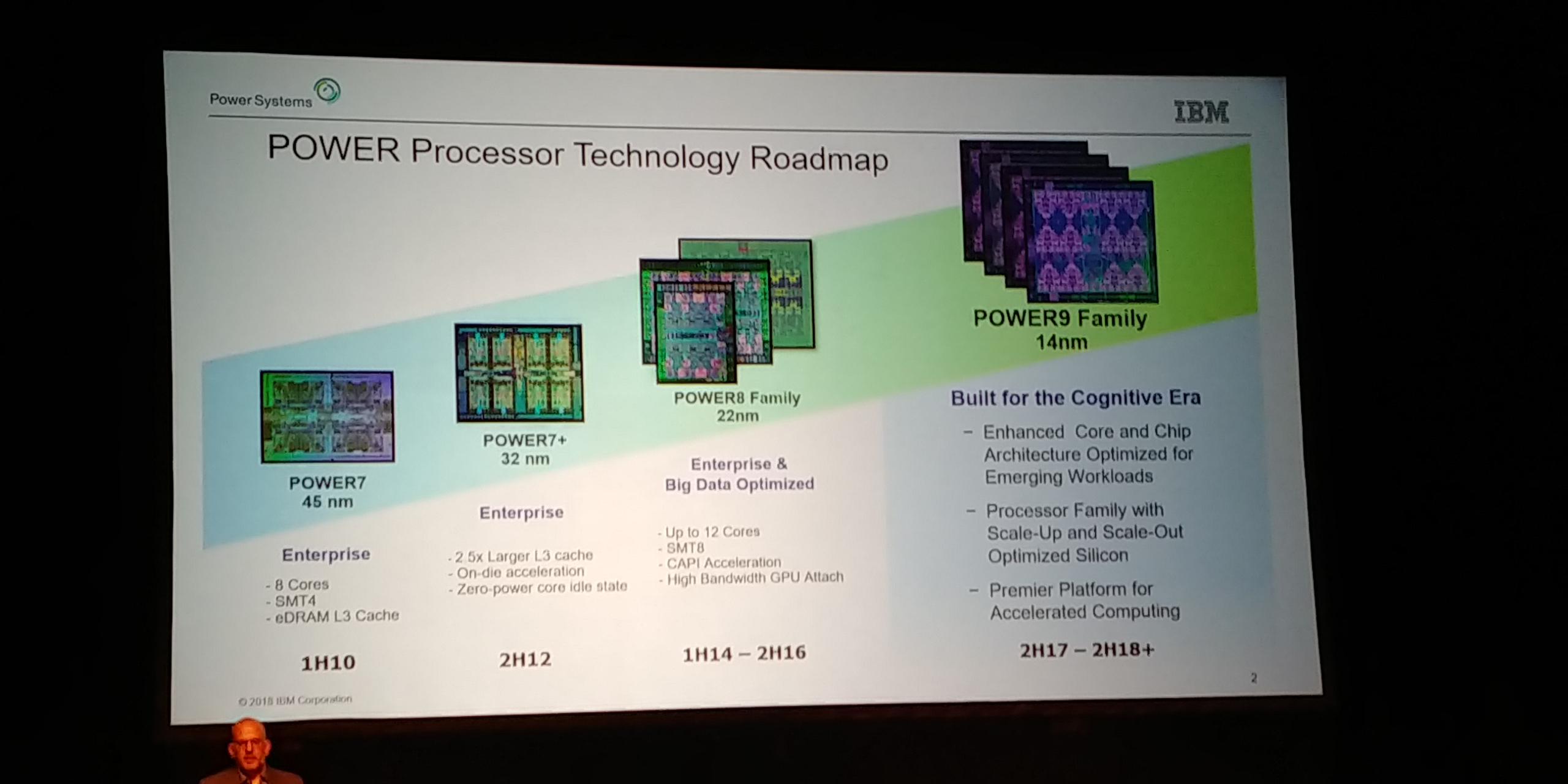
08:02PM EDT - Form slight variations of those designs to hit spots in the market
08:02PM EDT - First gen Power9 was two years ago at Hot Chips
08:02PM EDT - Deployed in the Summit Supercomputer
08:03PM EDT - That's built around 2-socket servers
08:03PM EDT - Today is the enterprise design, up to 16 socket
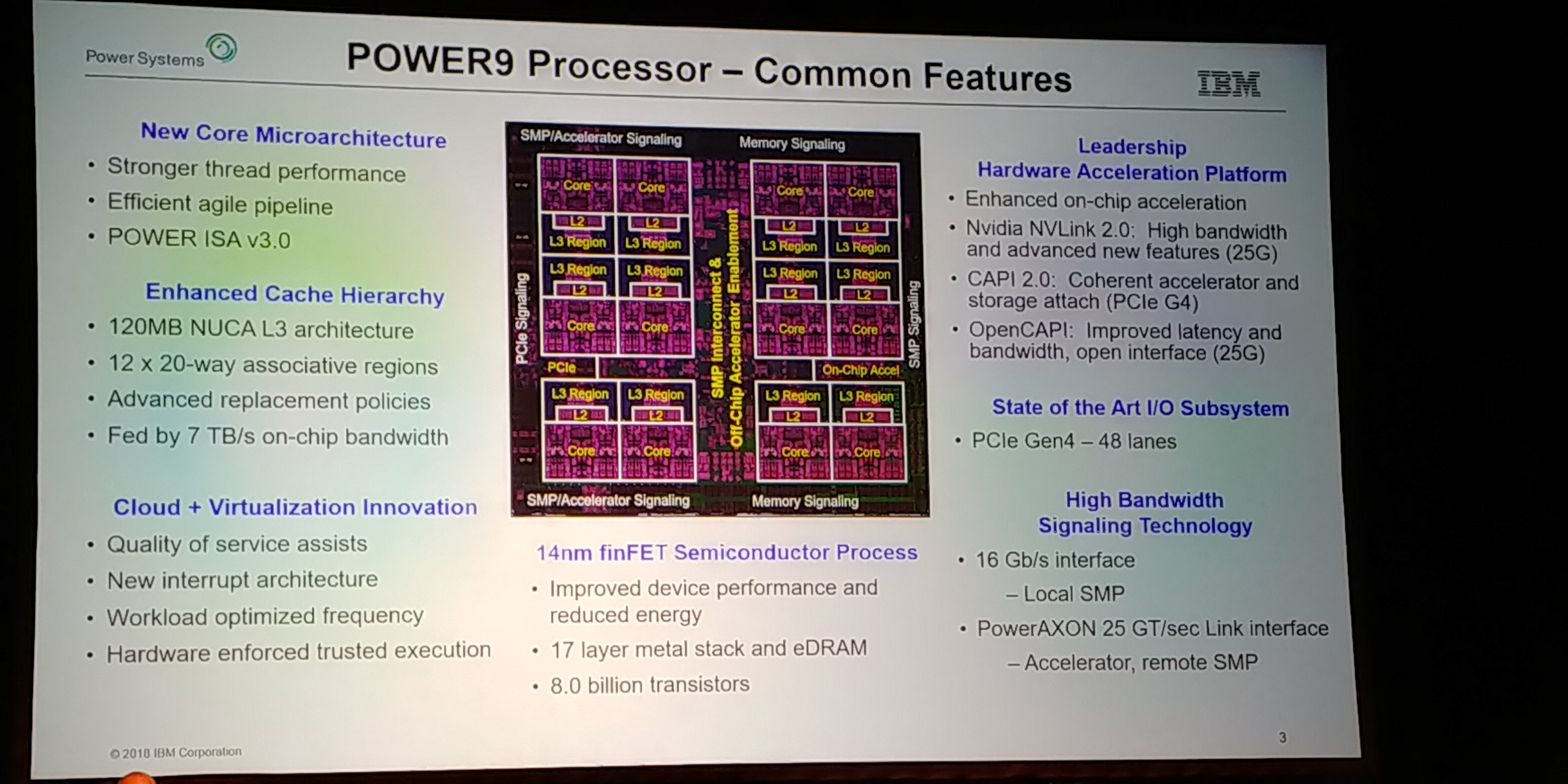
08:03PM EDT - Common features in all Power9 processors
08:03PM EDT - As we get more smaller transistors, same physical distance is actually further apart
08:04PM EDT - Couple of different variations of cores
08:04PM EDT - This is the Big core
08:04PM EDT - 8-way threading
08:04PM EDT - eDRAM for cache cells
08:04PM EDT - 120MB of on-chip L3
08:04PM EDT - 12x 20-way associative cache elements
08:04PM EDT - NUCA cache
08:04PM EDT - Fed by 7 TB/s on-chip bandwidth
08:05PM EDT - 8 billion transistors
08:05PM EDT - It would have taken 5 billion more transistors in traditional SRAM
08:05PM EDT - 14nm FF from GloFo
08:05PM EDT - 17 layer metal stack
08:05PM EDT - QoS
08:05PM EDT - Workload Optimized frequency
08:05PM EDT - Lots of perimeter IO to connect to devices
08:06PM EDT - NVLink 2.0 (25G), CAPI 2.0 (PCIe G4), OpenCAPI (25G)
08:06PM EDT - 48 lanes of PCIe Gen4
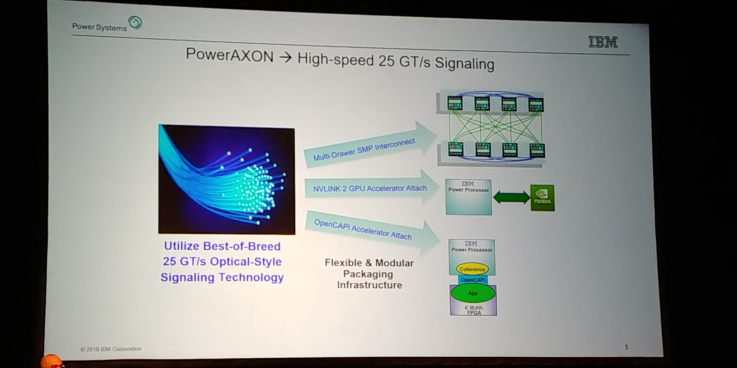
08:06PM EDT - PowerAXON 25 GT/sec Link for accelerators
08:06PM EDT - 'Reach out if you have an accelerator to attach to our CPUs'
08:07PM EDT - This is all common to the big Power9 chips
08:07PM EDT - PowerAXON is the new
08:08PM EDT - AXON stands for A and X (two types of SMP links), O for OpenCapi, N for NVLink
08:08PM EDT - Scale Up differs from current Scale Out CPUs
08:08PM EDT - More memory - 8 buffered channels for 230 GB/s, up from 150
08:08PM EDT - Up to 8TB per socket
08:08PM EDT - Better RAS, Compatible with Power8
08:09PM EDT - We want to connect memory via SERDES
08:09PM EDT - Can do this with Buffered Memory
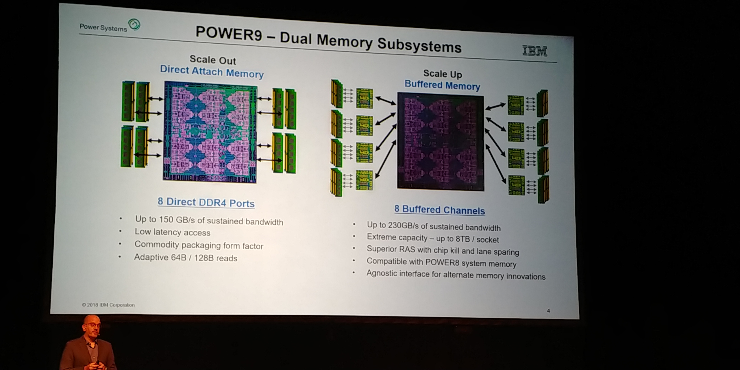
08:10PM EDT - The processor doesn't have to be built around DDR
08:10PM EDT - With DDR, you don't know if the write has completed as there is no acknowledgement. This can change with SERDES based implementations
08:11PM EDT - Can build a buffer for DDR4, DDR5, GDDR5, NRAM etc.
08:11PM EDT - See it as more important going forward
08:11PM EDT - Short range SERDES with active redrivers
08:12PM EDT - Drive it to GPUs (NVLink), CPU to CPU (SMP), or through OpenCAPI accelerator
08:12PM EDT - Customized for domain specific applications

08:13PM EDT - Scale Out is DDR based, Scale up is DMI based
08:13PM EDT - DMI is smaller silicon than DDR, so more room for PowerAXON
08:13PM EDT - More SMPs
08:14PM EDT - Swap out memory controllers
08:14PM EDT - Redrive memory controller, like a home agent bridge
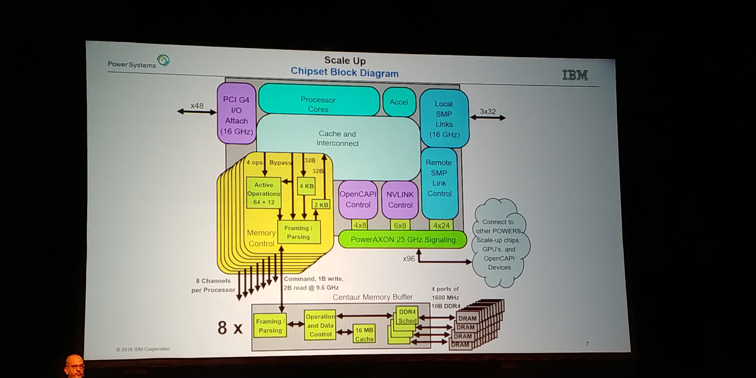
08:15PM EDT - Combine CPUs with Buffers, central to design
08:15PM EDT - aiming for reliability, baked into the buffers
08:15PM EDT - On-chip accelerators, g-zip, compression
08:15PM EDT - 3 links within motherboard for SMP
08:15PM EDT - remote SMP links that talk off board through AXON
08:16PM EDT - Logic blocks talk to different protocols
08:16PM EDT - A lot of the chip area is tied up in the PHYs or the interconnect, so adding all three doesn't add a lot of silicon die area
08:17PM EDT - (So PowerAXON can run OpenCAPI, NVLink, or SMP through one die block. It's bigger than a dedicated block, but it allows configurability depending on use)
08:17PM EDT - Centaur memory buffers
08:18PM EDT - DRAM devices are deterministic latency, e.g. 13 cycles, so DMI sends early tag in advance before checking CRC to line up muxes, so data can directly forwarded in expected time frame
08:19PM EDT - Needs to be built with this in mind
08:19PM EDT - Suggested systems
08:20PM EDT - four socket is easy - SMP to each CPU
08:20PM EDT - 16 socket is slightly different
08:20PM EDT - Get to any socket in two hops
08:21PM EDT - Power E980 Server box
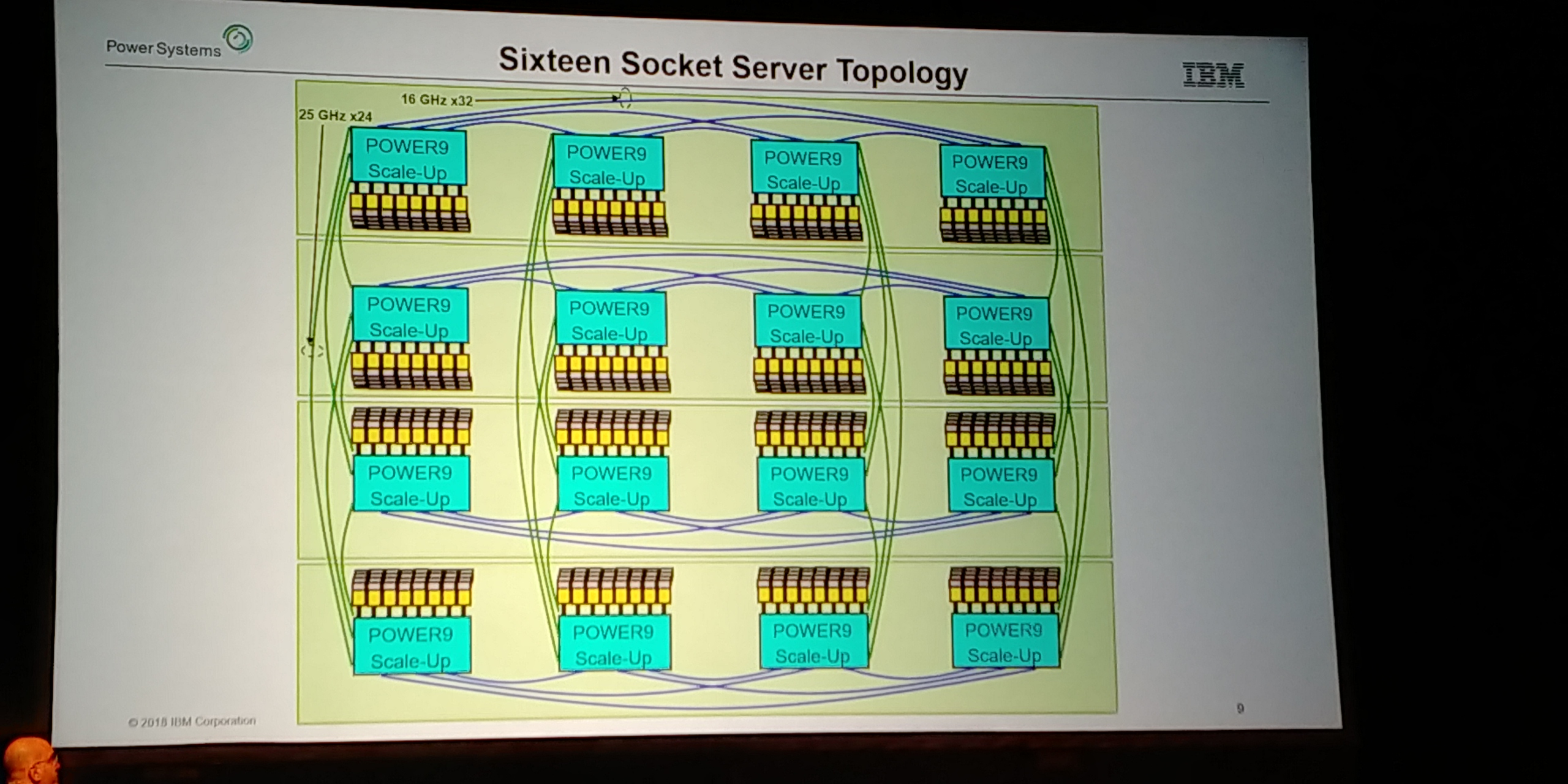
08:21PM EDT - Four sockets in 5 U
08:21PM EDT - 64TB of DRAM
08:21PM EDT - VRMs are redundancy
08:21PM EDT - Connectivity in the back
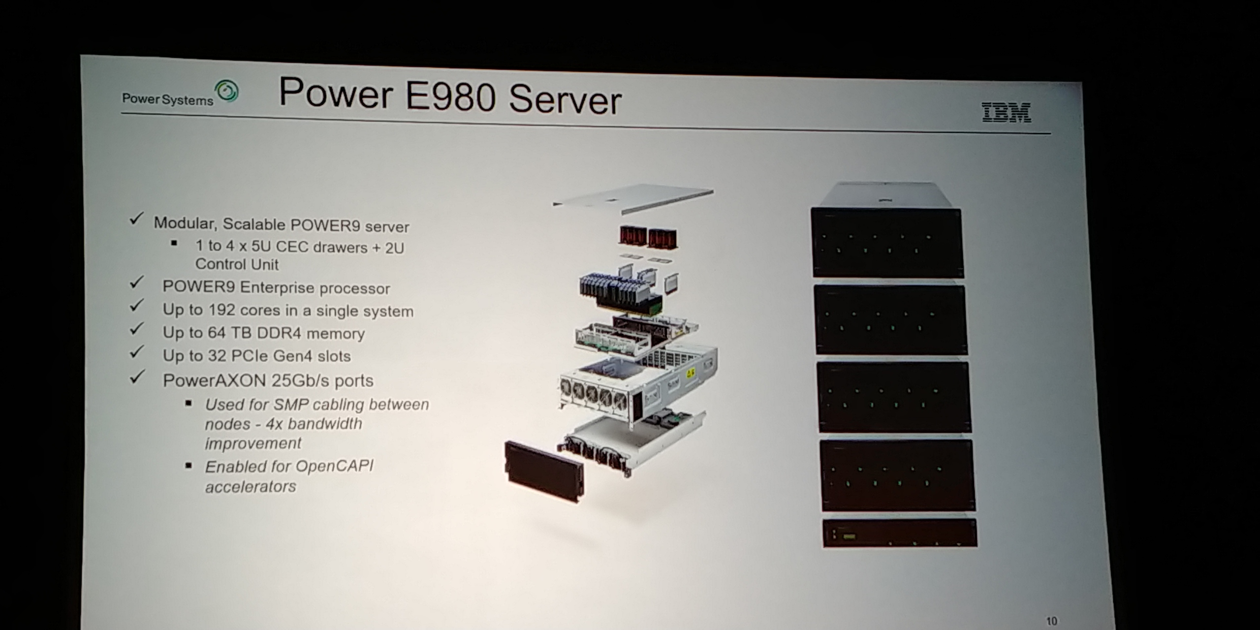
08:21PM EDT - 22U for 16-socket
08:21PM EDT - 8 PCIe devices
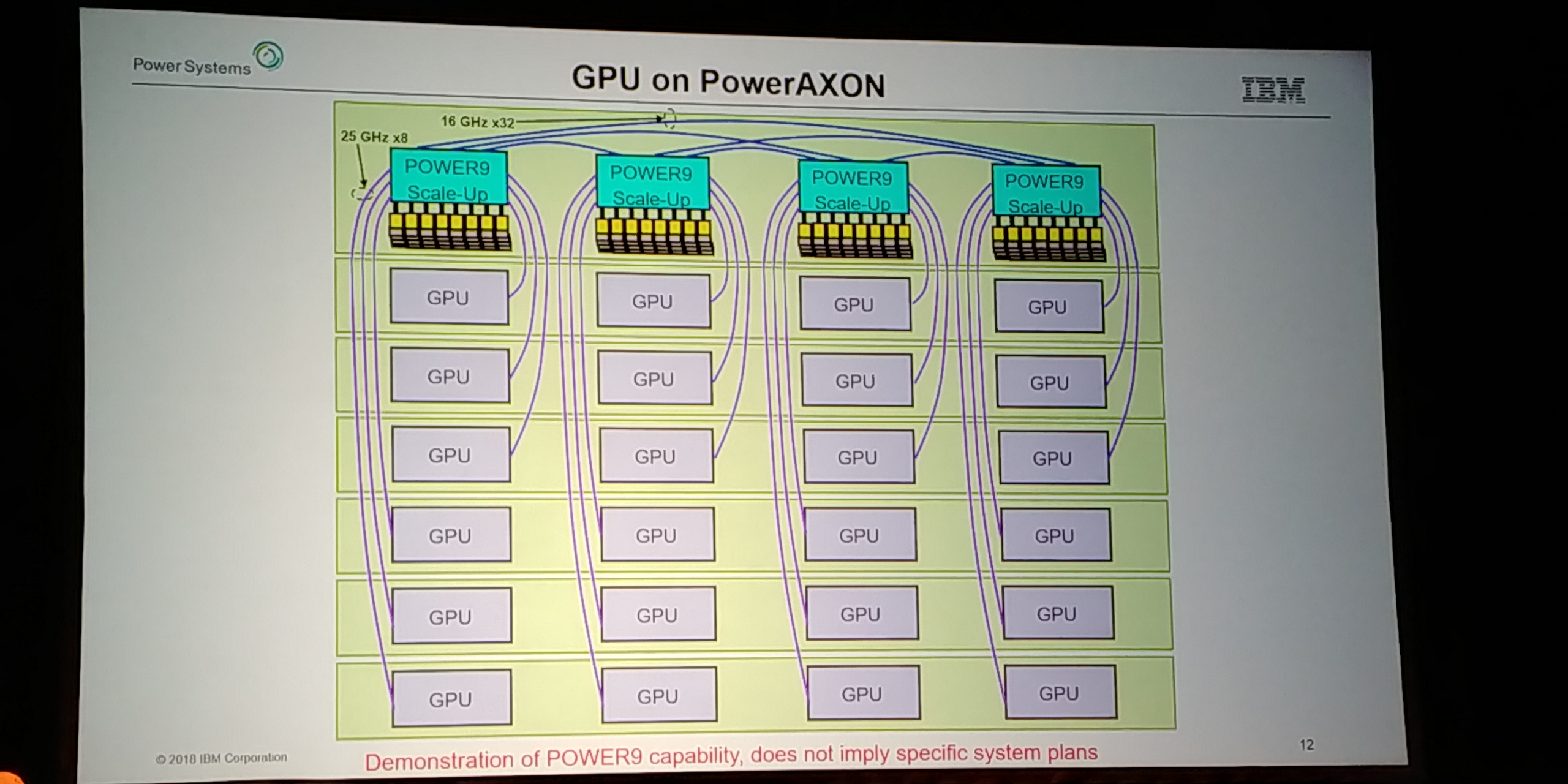
08:22PM EDT - GPU on PowerAXON example
08:22PM EDT - Plug an array of GPUs on NVLink alongside SMP
08:22PM EDT - Future
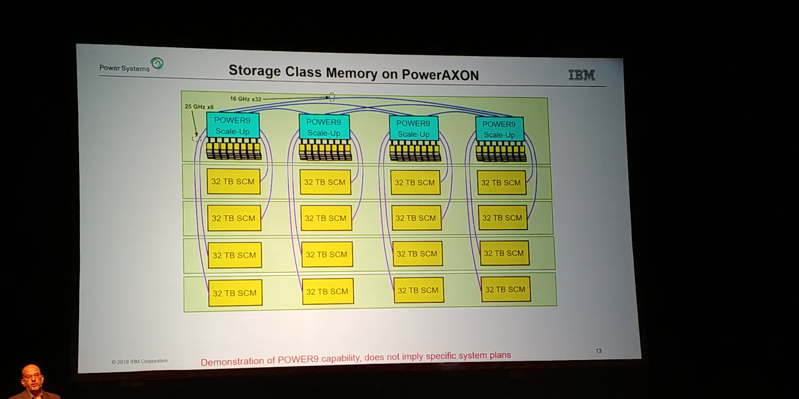
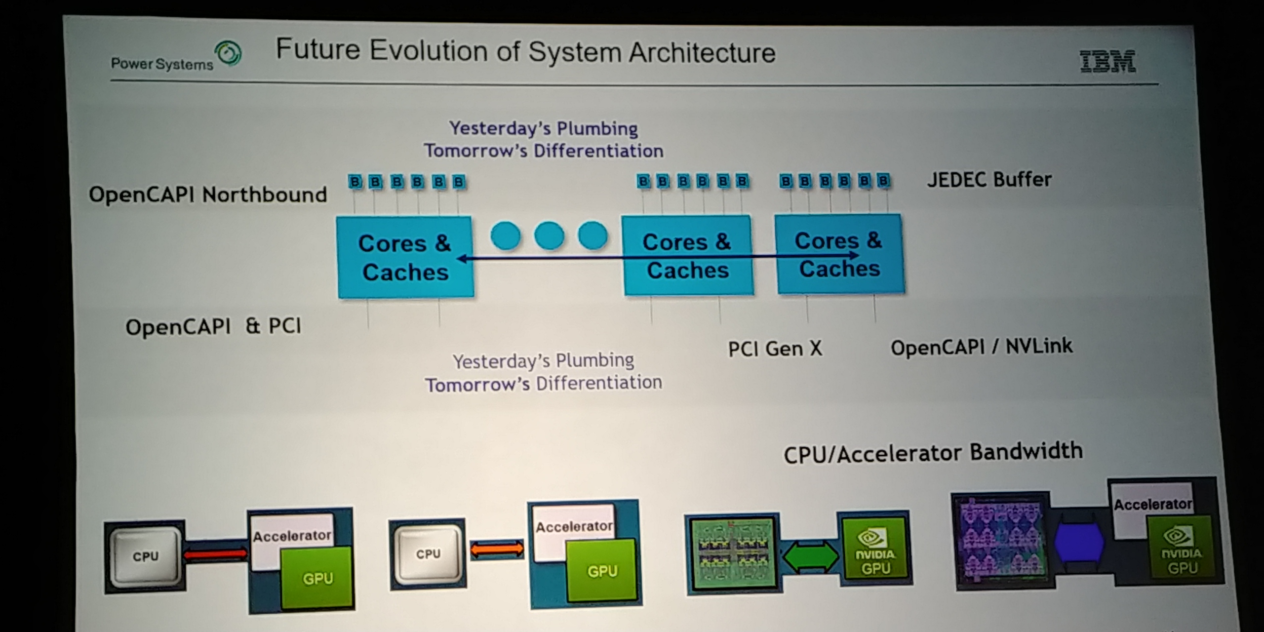
08:23PM EDT - One PHY to rule them all
08:23PM EDT - One connector for SMP, OpenCAPI, NVLINK
08:23PM EDT - Future is based on open standard buffer
08:23PM EDT - for memory over AXON
08:23PM EDT - 4 x bandwidth vs DDR4
08:24PM EDT - OpenCAPI target of 5ns
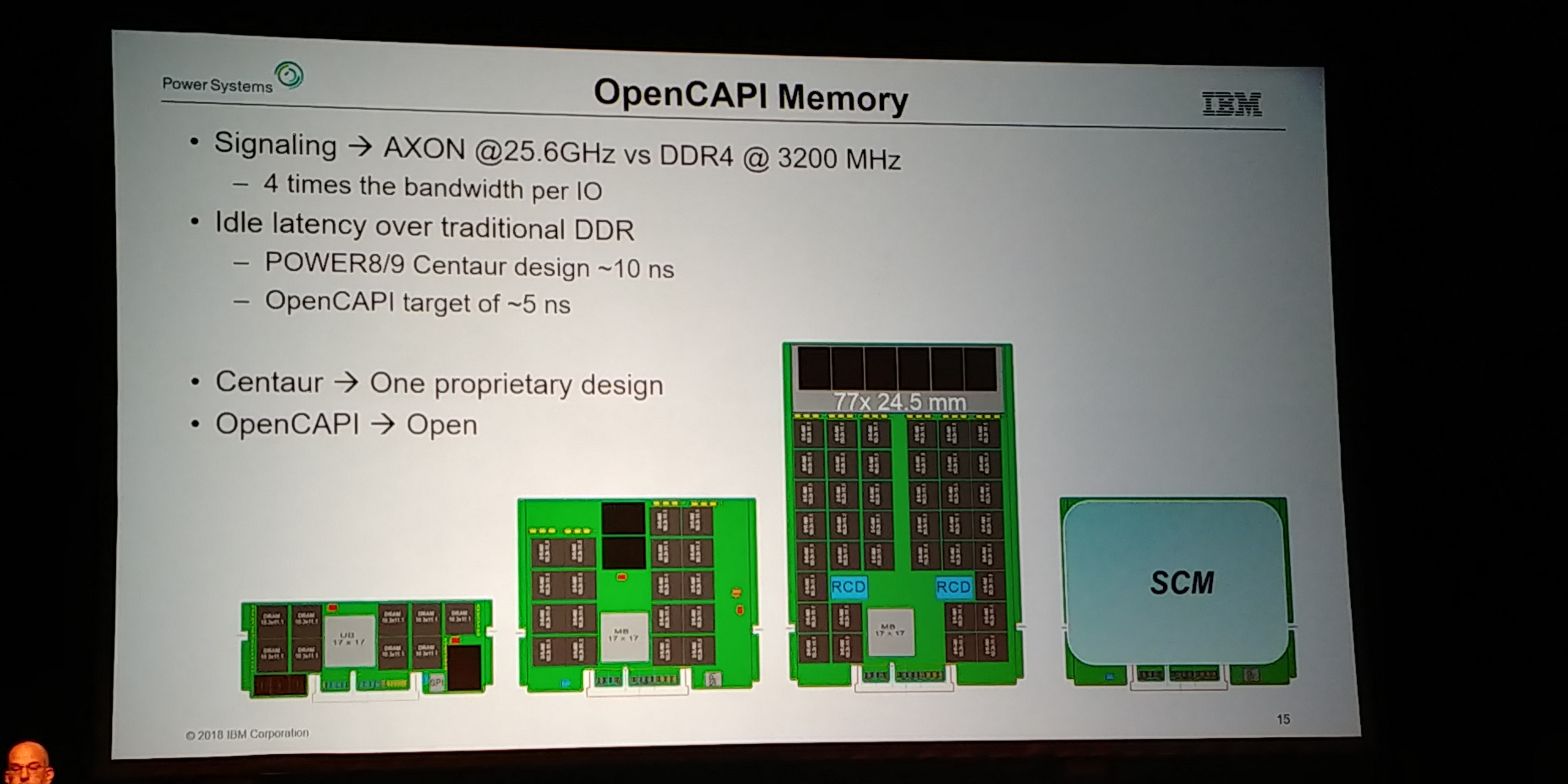
08:24PM EDT - Big tall DIMMs
08:24PM EDT - Targeting 5ns idle latency
08:24PM EDT - new buffer is a smaller chip - single port with single buffer
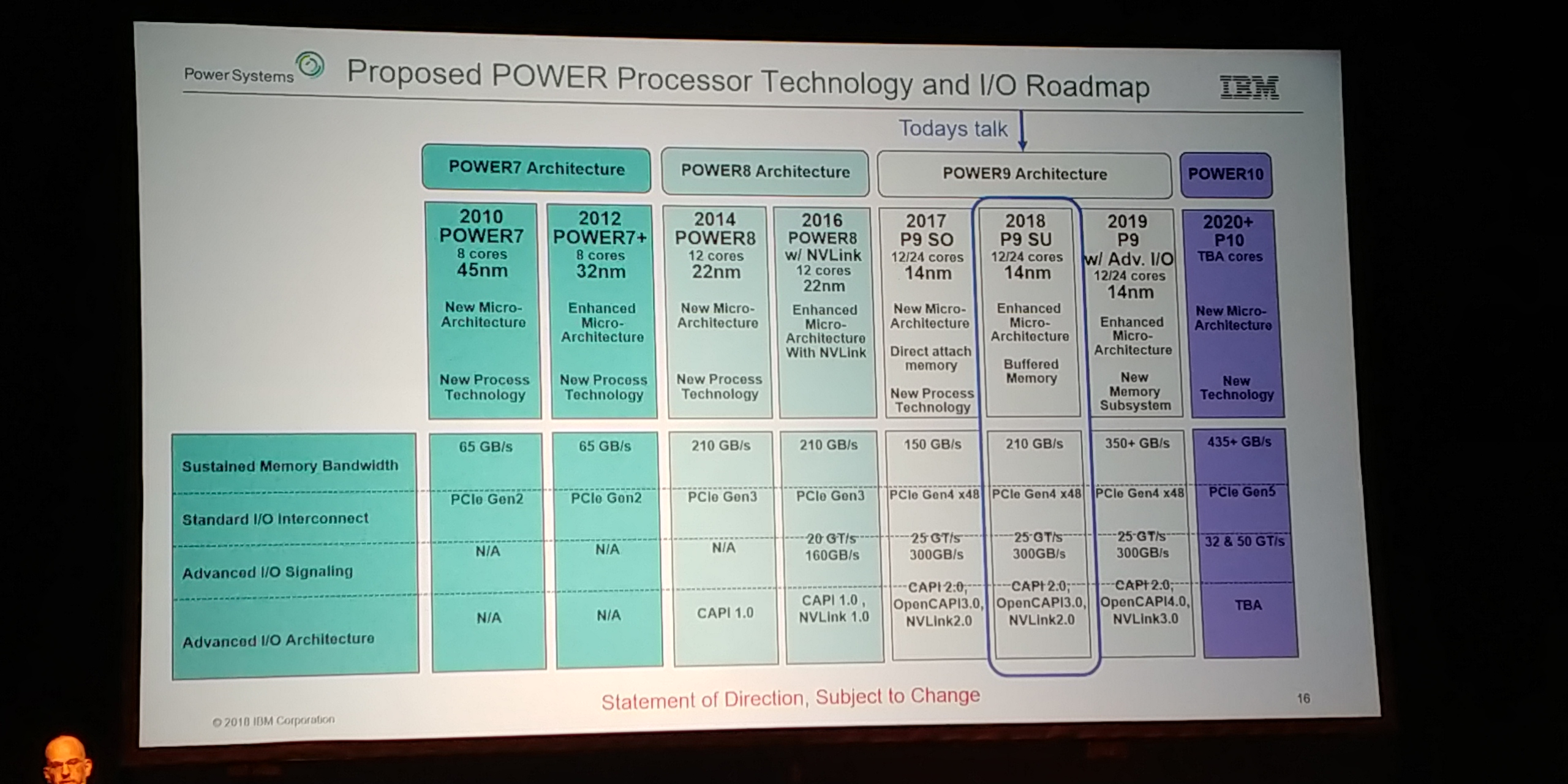
08:25PM EDT - Next Power9 chip with new memory technology on AXON and CAPI
08:25PM EDT - Up to 350 GB/s
08:25PM EDT - OpenCAPI 4.0
08:26PM EDT - Power10 on DDR5, up to 435GB/s on memory
08:26PM EDT - 2020+
08:26PM EDT - Q&A
08:27PM EDT - Q: We designed POWER with GPU. Didn't work with NVLINK, connecting to GPU by little-endian? A: Yes, we support both, and mixed
08:28PM EDT - Q: Power Delta on SERDES? A: Different because never idle. Based on lane count. Power in processor socket is lower at full bandwidth. From a power perf POV is great
08:29PM EDT - Only in low utilization would it be iffy
08:29PM EDT - Buffer is a handful of watts
08:29PM EDT - Q: Area of chip? A: 600-ish mm2
08:29PM EDT - Q: Latency impact of eDRAM cache? A: Minimal
08:30PM EDT - Q: Shipping? A: 2-socket was last year, these new boxes were just announced. Shipping over next few months
08:30PM EDT - Next talk is Fujitsu: https://www.anandtech.com/show/13258/hot-chips-2018-fujitsu-afx64-arm-core-live-blog


1 Comments
View All Comments
Yojimbo - Tuesday, August 21, 2018 - link
Well, it was to be expected, but I guess they nigh on confirmed that NVIDIA is coming out with a data center GPU in 2019. I think there's only a very small chance a new NVLink version would be completed and integrated with an IBM CPU die much before a GPU with it came out.