TSMC’s Fab 14B Photoresist Material Incident: $550 Million in Lost Revenue
by Anton Shilov on February 20, 2019 8:30 AM EST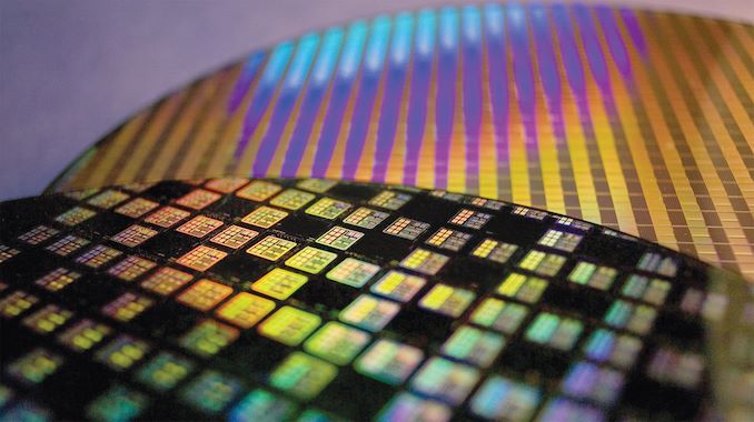
TSMC on Friday revealed more details regarding an incident with a photoresist material at its Fab 14B earlier this year. The contaminated chemical damaged wafers on TSMC’s 12 nm and 16 nm lines, and the company now expects the full impact of the event to reduce their revenue by a whopping $550 million in the first quarter.
TSMC said that a batch of photoresist it used included a specific element which was abnormally treated, creating a foreign polymer in the photoresist. The problem was detected late when the wafer yeilds were lower than expected. As it turns out, consequences of the photoresist incident at Fab 14B were more serious than initially calculated by TSMC. There are media reports claiming that between 10,000 and 30,000 wafers were affected and had to be scrapped, but TSMC has never confirmed either of the numbers.
According to media reports, the affected companies include HiSilicon/Huawei, NVIDIA, and MediaTek, but TSMC has not disclosed names of its customers that suffered from the incident. The only thing that TSMC does confirm is that it has already negotiated new delivery scheduled with its customers.
In any case, the cost of the wafers totals $550 million and they will be made up in Q2. In the meantime, TSMC is pulling in "certain production" from Q2, which will bring in $230 million in additional revenue in Q1. As a result, TSMC’s first quarter earnings are now expected to be between $7 billion and $7.1 billion, down from $7.3 - $7.4 billion predicted in mid-January.
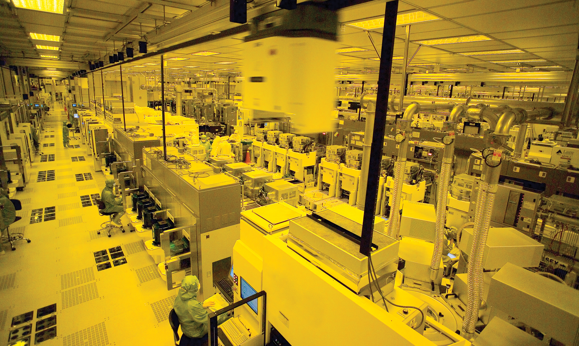
In a bid to avoid similar situations in the future, TSMC will make inspection of incoming materials more thorough and will strengthen inline wafer inspection. The company also indicated that it will need better controls because of increasing complexity of leading-edge fabrication technologies.
Related Reading:
- TSMC Chip Yields Hit By Bad Chemical Batch
- TSMC: 7nm Now Biggest Share of Revenue
- TSMC: Outbreak of Malware That Triggered Delays & Losses Caused by Software for New Tool
- TSMC: First 7nm EUV Chips Taped Out, 5nm Risk Production in Q2 2019
Source: TSMC


29 Comments
View All Comments
Gunbuster - Wednesday, February 20, 2019 - link
TLDR: Factory worker screws up a jug of chemical. TSMC tossed the jug into their machines with no QC. Half a billion $ poof gone.repatch - Wednesday, February 20, 2019 - link
No, no poof. This article has a horrible title. $500 million is lost in the first quarter true, but it'll be made up in the second (which the article does say). After all, that $500 million in business won't just move to the next fab overnight for production. Changing fabs is extremely hard. Yes, SOME business MIGHT be lost, since late delivery might mean some reduction in volume, but it'll be pretty small. Also, the actual product they lost will cost something, but nowhere near the $500 million figure. HORRIBLE title.Sahrin - Saturday, February 23, 2019 - link
...no, it’s not. Until TSMC negotiates and delivers the wafers at 100% of the initial price, the revenue is gone.The article title is 100% true. If TSMC is actually able to secure the production at 100% of the price, then you are still wrong - the tools and fab have a defined useful life, and it’smeasured in wafers produced - these wafers were bout and scrapped, which is a real loss not just in revenue but in the cost of producing the wafers themselves.
HORRIBLE comment.
Morawka - Sunday, February 24, 2019 - link
Well TSMC has lowered their guidance by 3 Billion so you calculate the real cost.happily1986 - Wednesday, February 20, 2019 - link
Wrong!Fact 1: Resist are not charged into Lithography foster tools in Jugs. The most common means is via bottles.
Fact 2: Resist was already compromised when it arrived from the realist supplier hence the stated corrective action was to enforce stricter inspection of of incoming material ie IQC
Manch - Wednesday, February 20, 2019 - link
jug vs bottle...splitting hairs much? LOLLMonty - Wednesday, February 20, 2019 - link
I wonder if any of this will be covered by insurance.Since I'm eagerly awaiting Zen 2, I'm glad AMD wasn't affected. 🙂
Xajel - Wednesday, February 20, 2019 - link
AMD doesn't use 16nm process, they use 14nm and 12nm they already use GloFo. And the second source is Samsung (as GloFo licensed these two from Samsung, so for AMD little work to do to switch between the two). As for TSMC, the only process currently in use by AMD is the 7nm process which if these news are to be taken is not affected by the contamination.WinterCharm - Wednesday, February 20, 2019 - link
Yeah, this was a near miss for AMD.trane - Wednesday, February 20, 2019 - link
PS4 Slim/Pro; Xbox One S/X SoCs are all fabbed at TSMC 16FF+. Those actually might be AMD's highest volume products. Granted, it's a co-development between AMD and Sony/Microsoft, so not quite the same.