Hot Chips 31 Live Blogs: NVIDIA Multi-Chip AI Accelerator at 128 TOPS
by Dr. Ian Cutress on August 20, 2019 1:55 PM EST- Posted in
- Artificial Intelligence
- Hot Chips
- NVIDIA
- Live Blog
- DNN
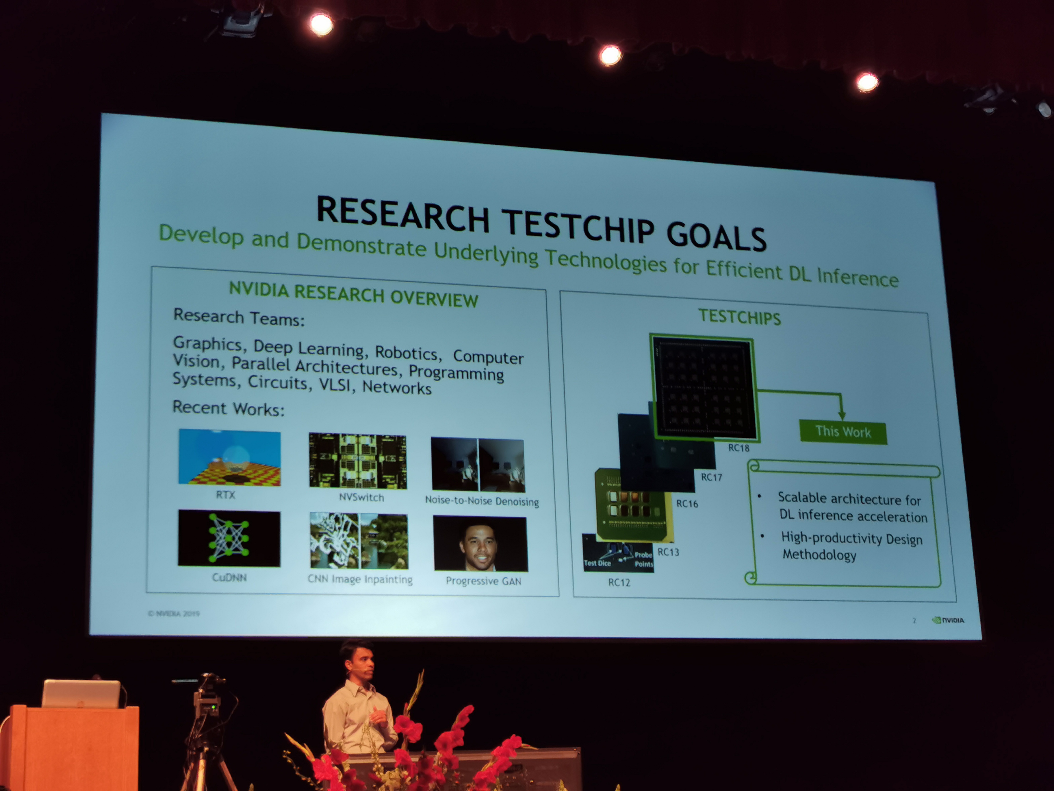
02:04PM EDT - NVIDIA announced at a VLSI conference last year that it had designed a test multi-chip solution for DNN computations. The company is explaining the technology today at Hot Chips, with the idea that what they've created could be a stepping stone for future monetizable products.
02:04PM EDT - This is a test chip
02:04PM EDT - NVIDIA research does many test chips every year
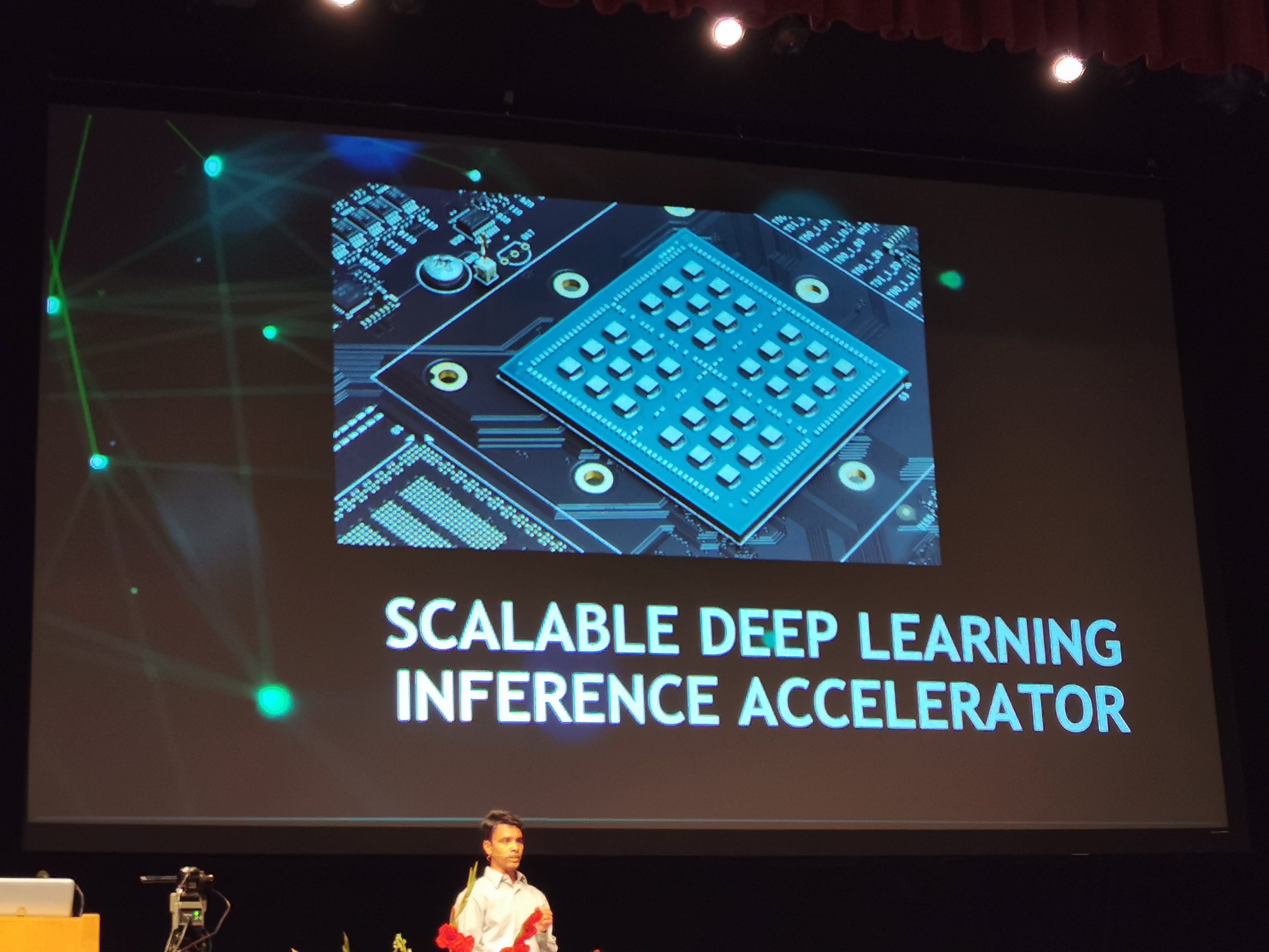
02:05PM EDT - This work is about multi-chip DL inference
02:05PM EDT - CNN was a target for this test chip
02:06PM EDT - System is configurable for scale
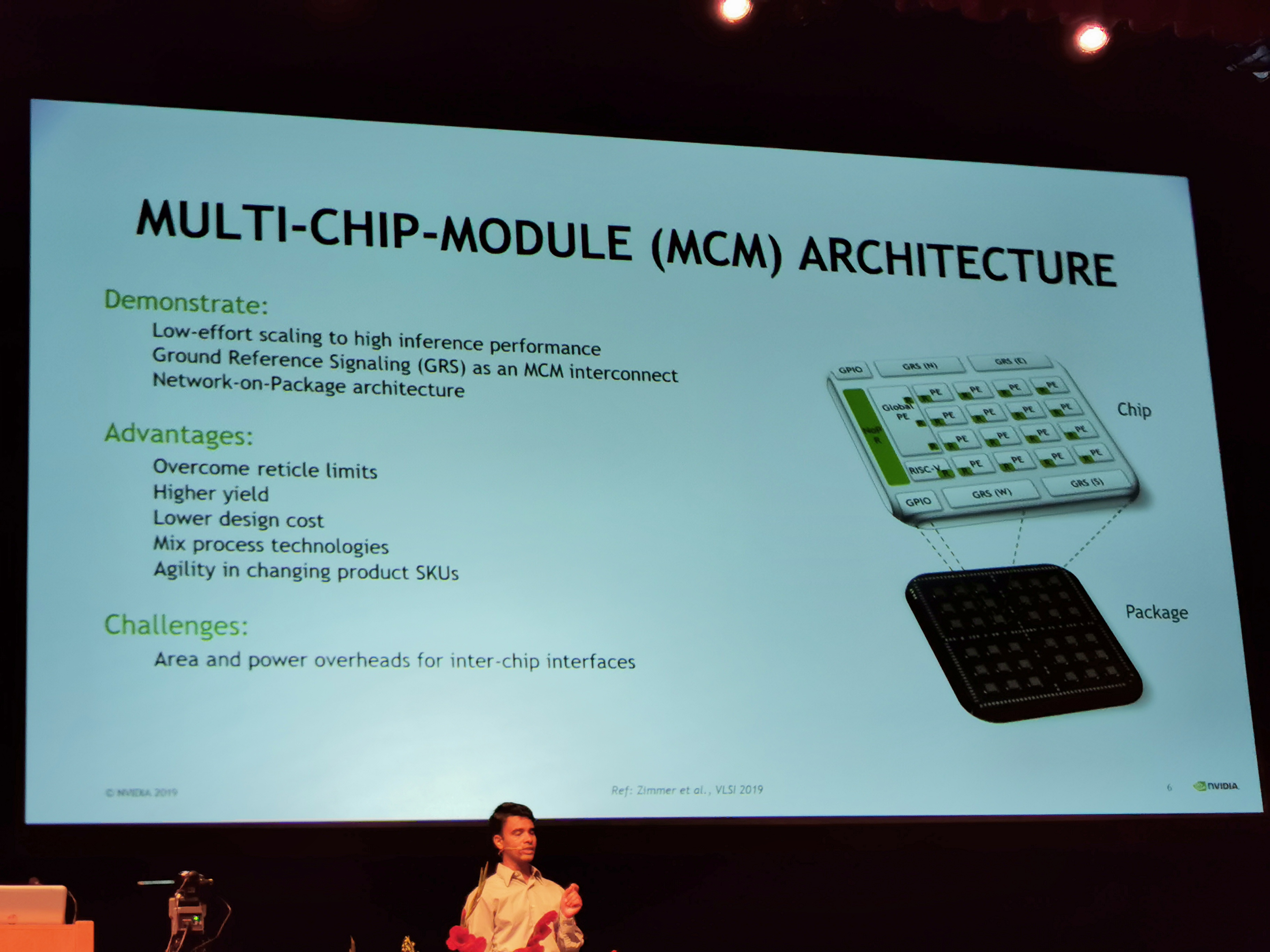
02:09PM EDT - 36 small chips
02:09PM EDT - large scale inference accelerators
02:09PM EDT - three key objectives
02:09PM EDT - high inteference scaling and perfomrance
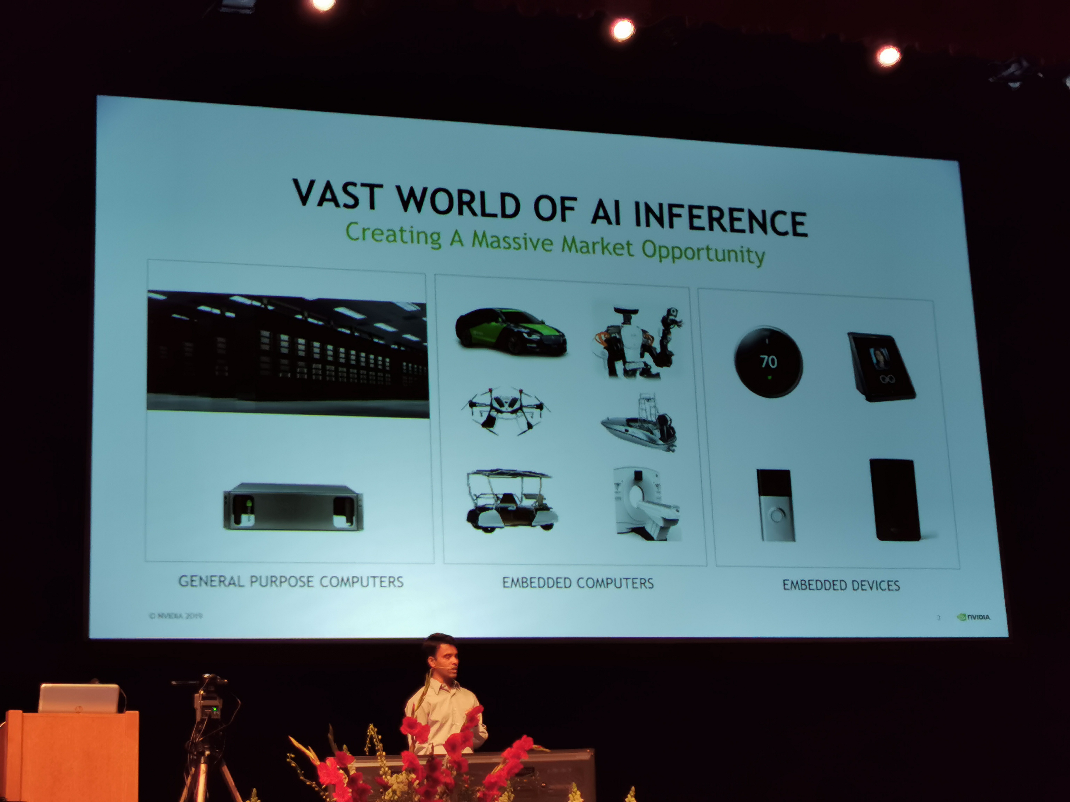
02:09PM EDT - each chip could be a DL edge inference accelerator
02:09PM EDT - many chips enabled data-center scale throughput
02:09PM EDT - network on package architecture
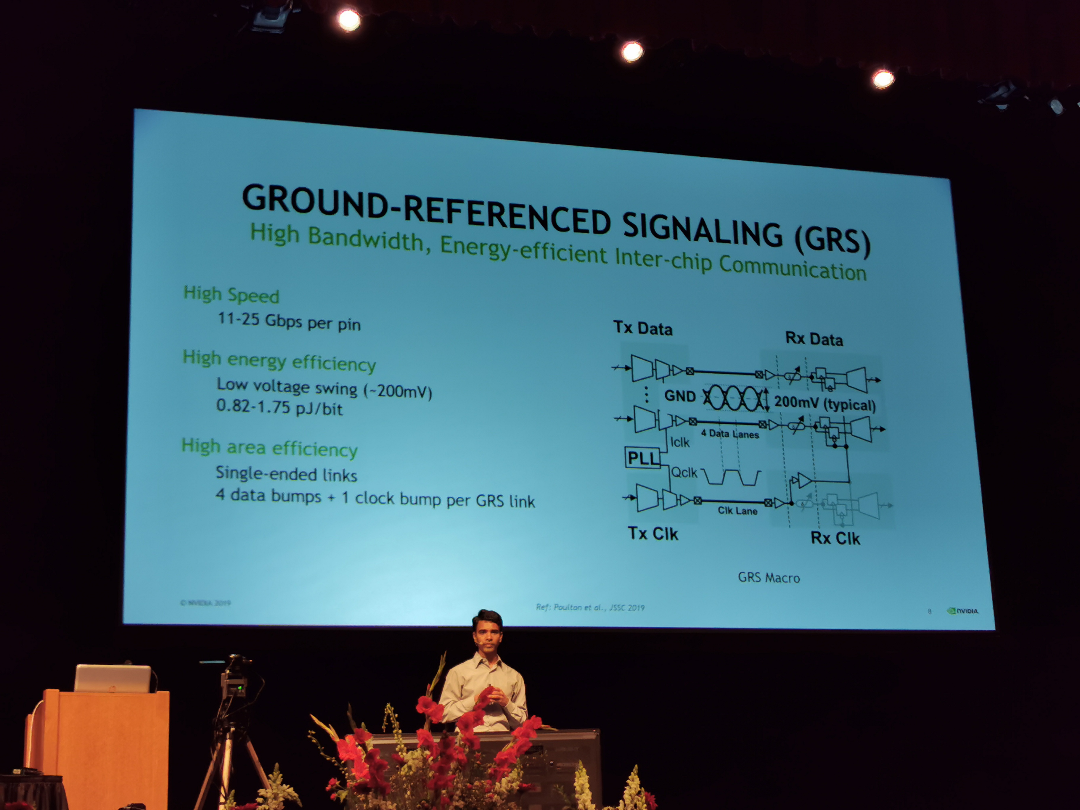
02:10PM EDT - Ground Reference Signalling as an MCM interconnect
02:10PM EDT - Chiplet Enables reuse and lower cost
02:10PM EDT - Assemble existing chips together
02:10PM EDT - NOC uses RISC-V
02:10PM EDT - 20ns per hop
02:10PM EDT - Network on chip and network on package
02:11PM EDT - Ground Reference Signalling - low voltage signalling, up to 1.75 pJ/bit, up to 25 Gbit per pin
02:11PM EDT - Single ended links
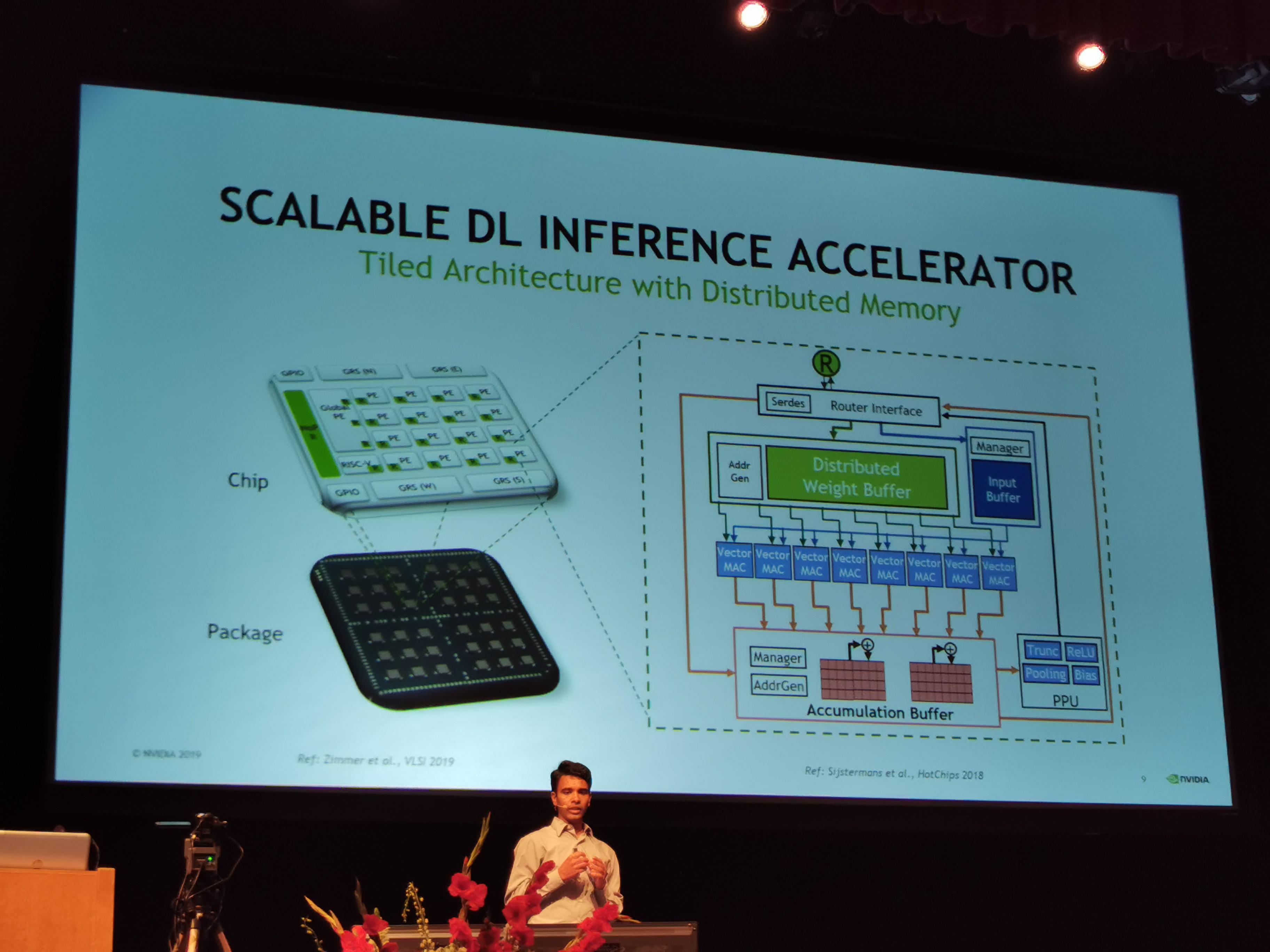
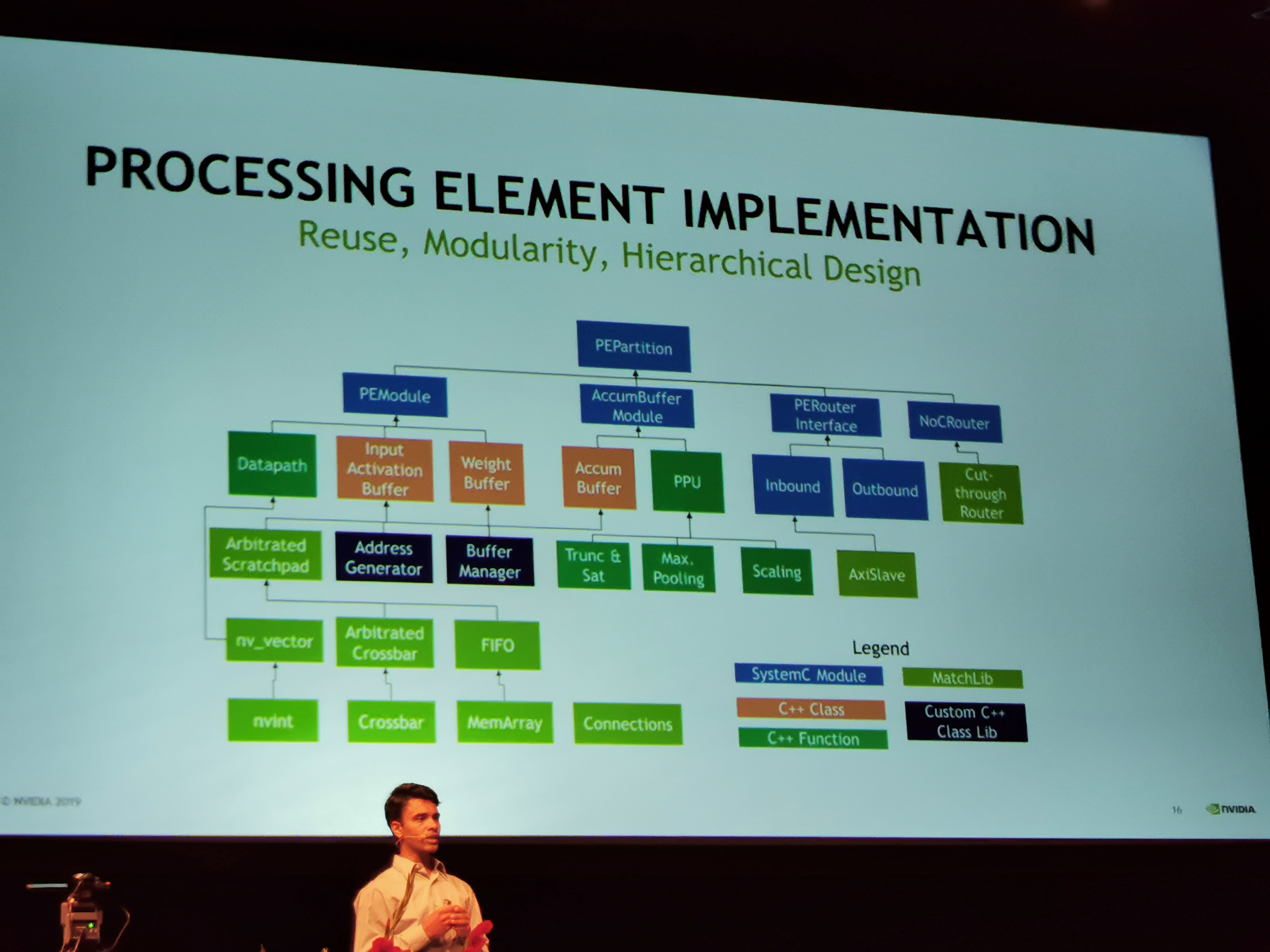
02:12PM EDT - Tiled Architecture with Distributed Memory
02:12PM EDT - RISC-V controller is a chip controller
02:13PM EDT - 8 Vector MACs per PE
02:13PM EDT - Processing Engine
02:13PM EDT - Each chip is 12 PEs, Each package is 6x6 chips
02:14PM EDT - PE - 8 MACs, chip is 96 MACs, package is 3456 MACs
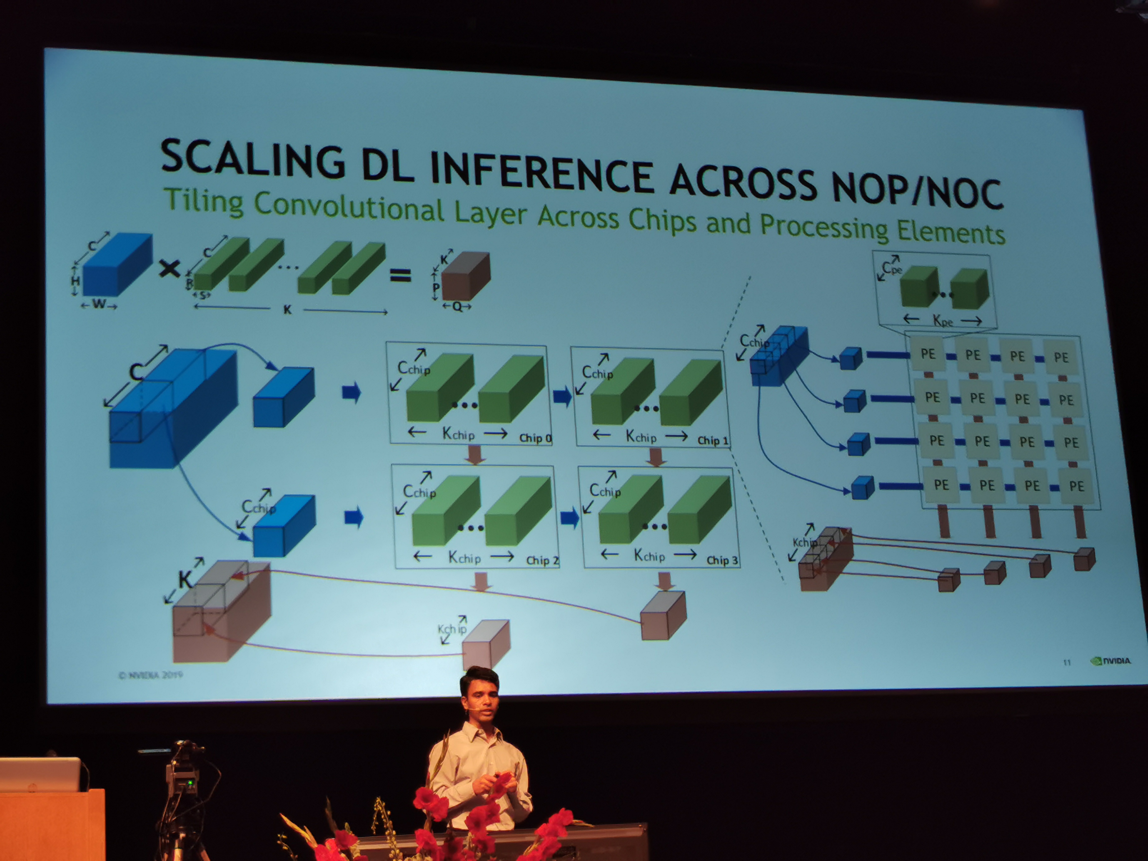
02:15PM EDT - Designed for CNNs
02:15PM EDT - Can do different tiling strategies

02:17PM EDT - Multicast support
02:17PM EDT - Extracting model parallelism using the NoP and NoC
02:18PM EDT - TSMC 16mm, 2.5mm x 2.4mm each
02:18PM EDT - 100 Gbps per link
02:18PM EDT - 9.5 TOPS/W, 128 TOPs
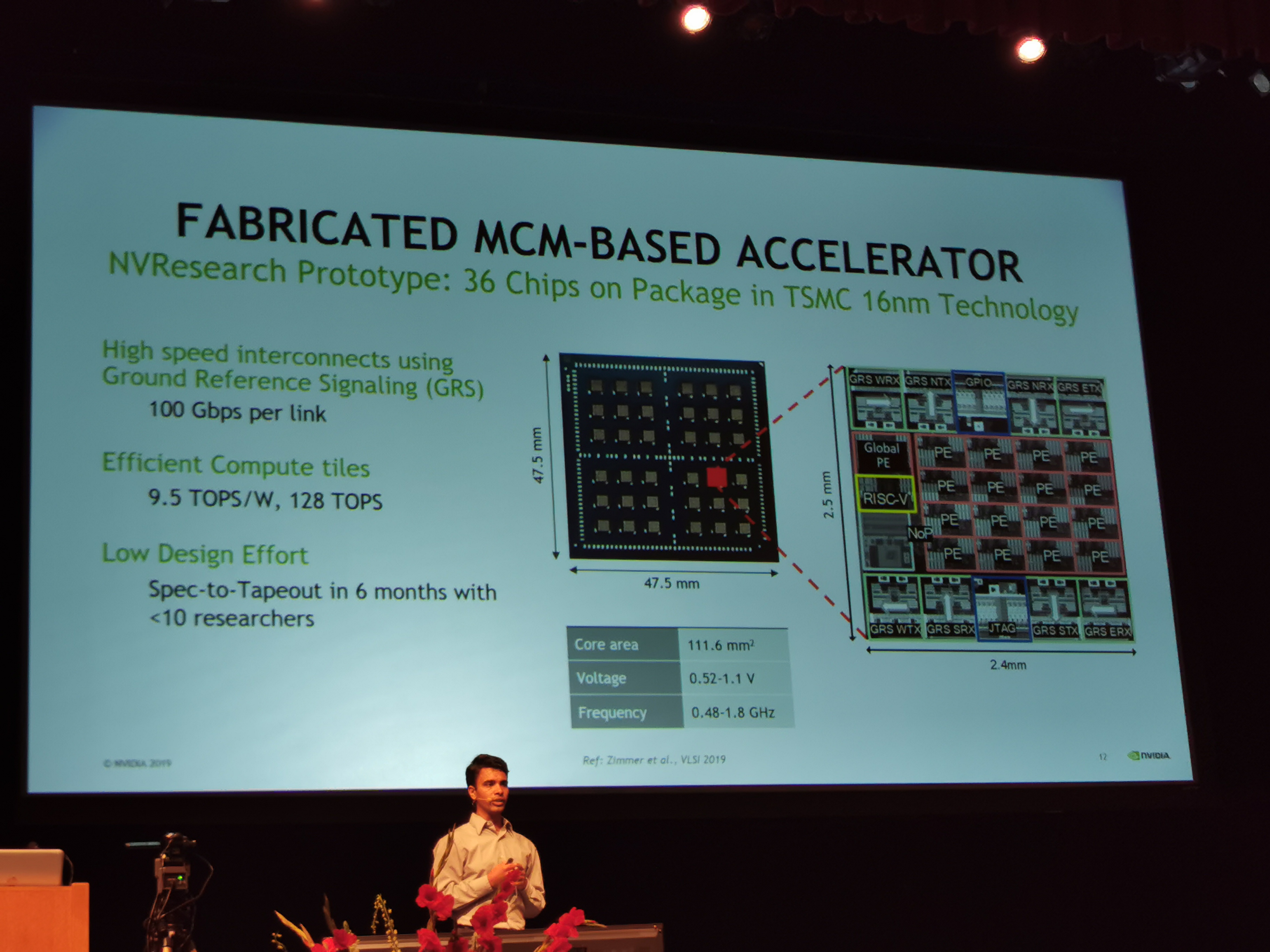
02:18PM EDT - 6 months from spec to tapeout
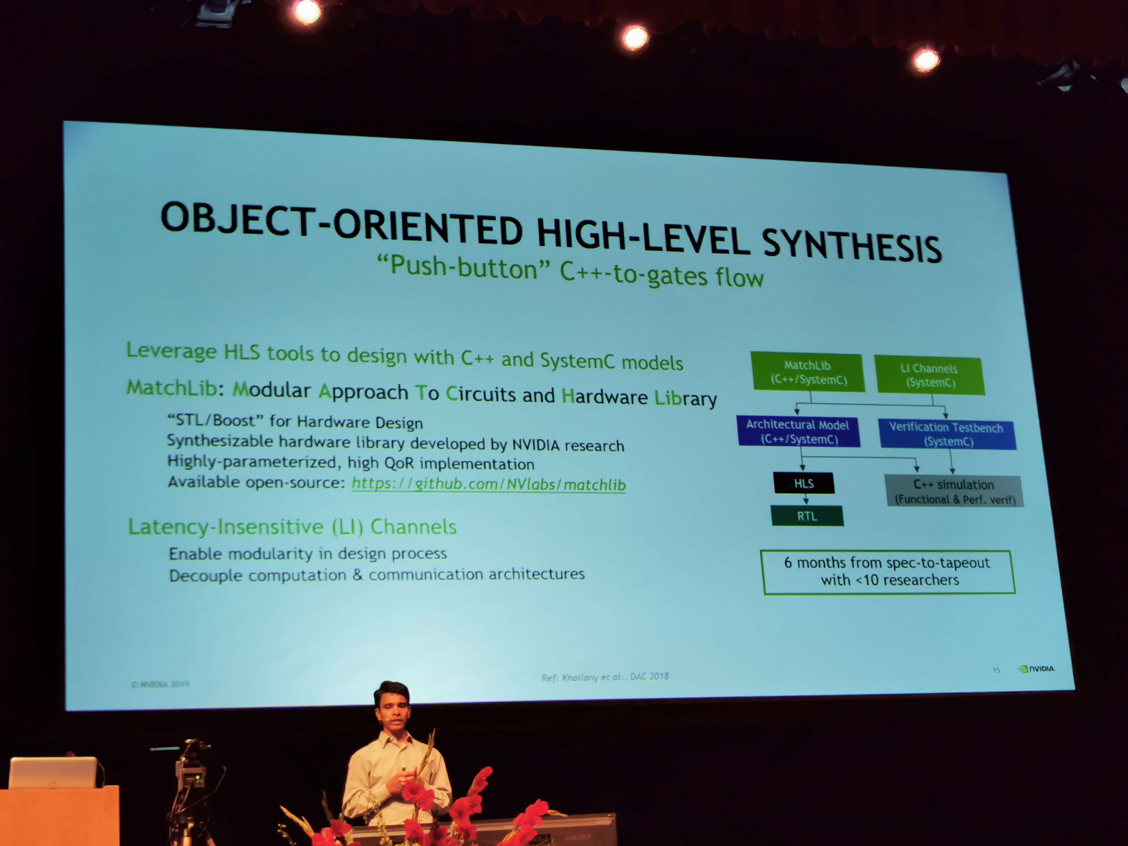
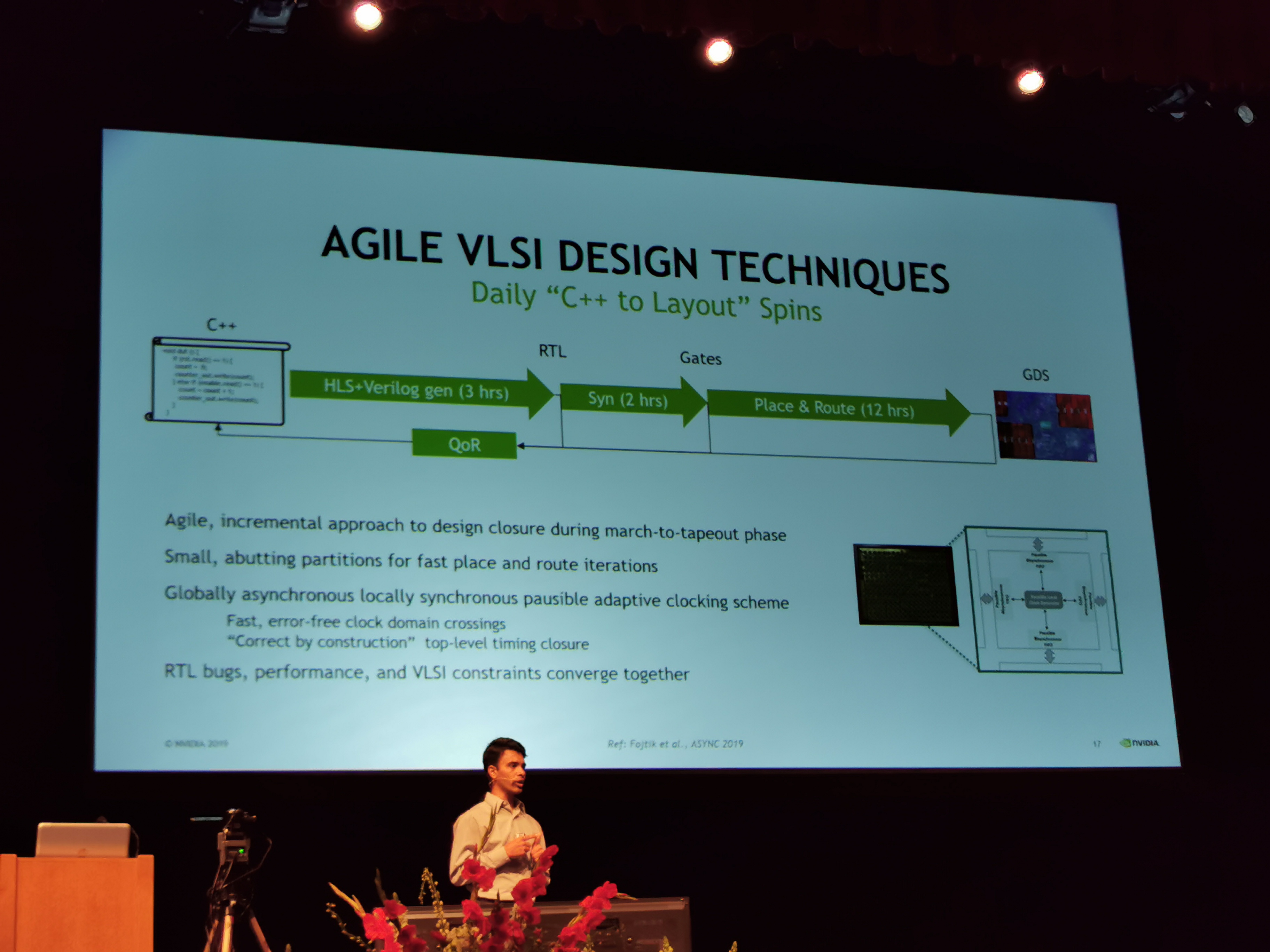
02:19PM EDT - Designed in high level synthesis
02:19PM EDT - Agile VLSI Design
02:19PM EDT - Continuous integration with automated tool flows
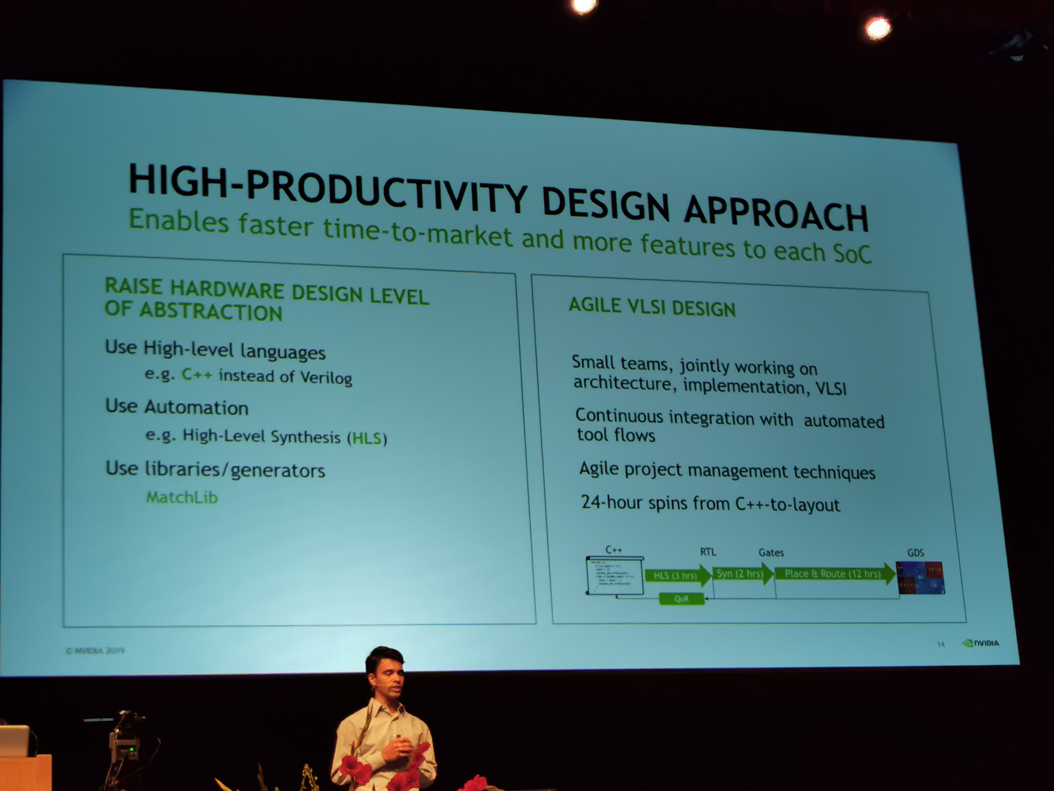
02:20PM EDT - C++ to Gates design in 12 hours
02:20PM EDT - MatchLib is opensource
02:24PM EDT - Experimental results
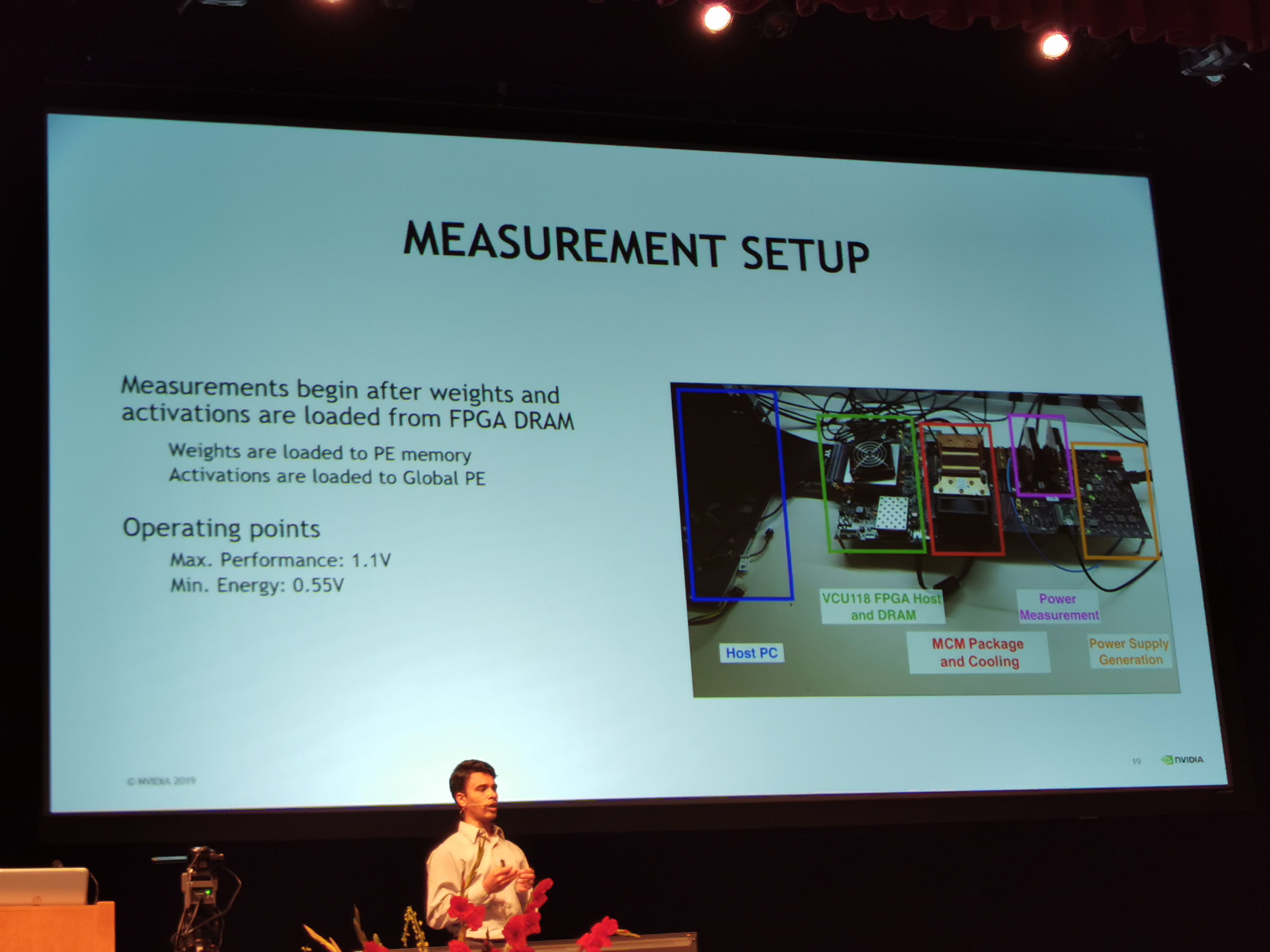
02:24PM EDT - Custom PCB with FPGA DRAM
02:25PM EDT - 27x improvement with 32 chips
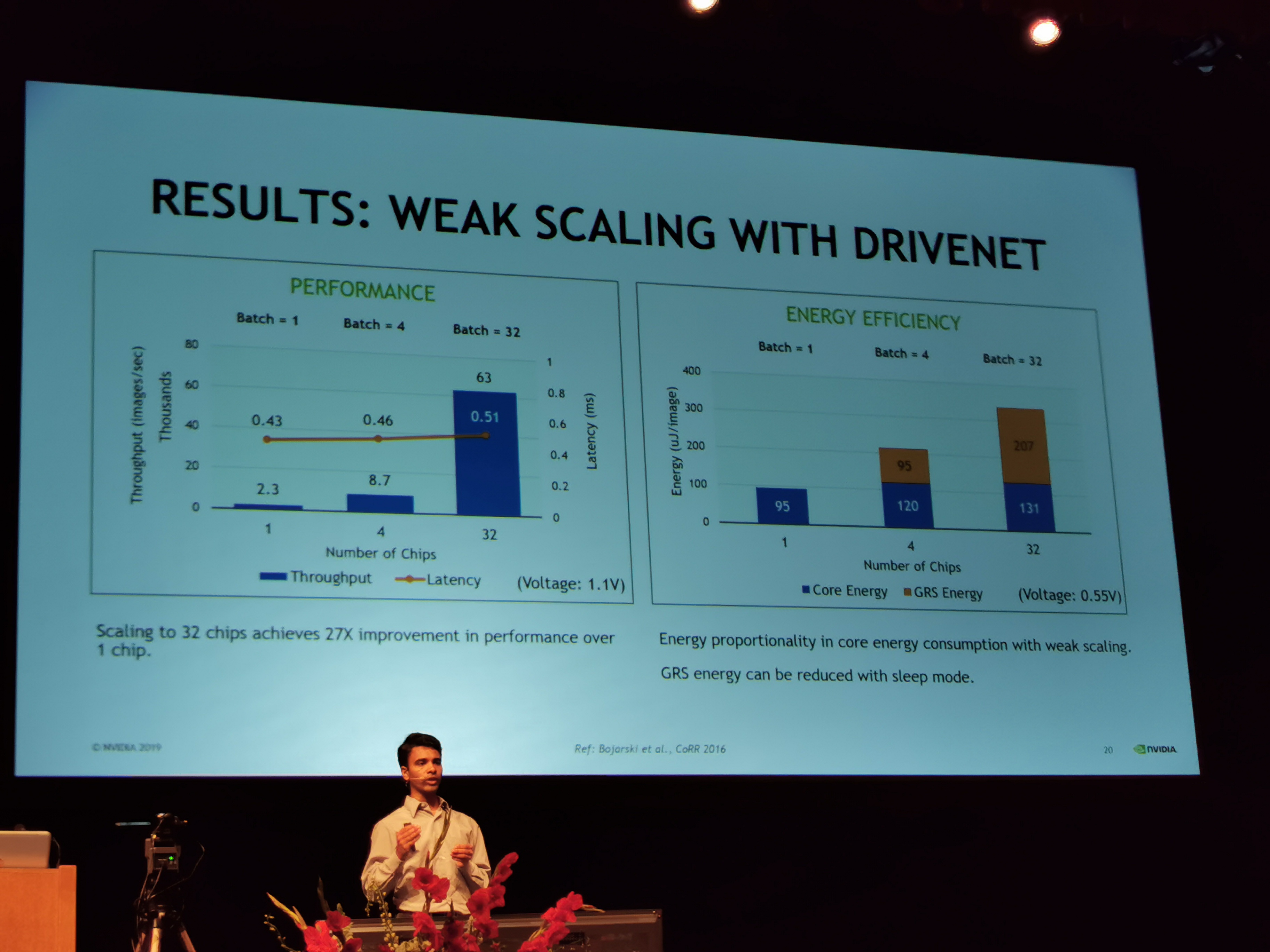
02:25PM EDT - GRS uses most energy at high chip counts
02:25PM EDT - (oh that energy is per image)
02:26PM EDT - At high batch, GRS links are all active all the time, consuming power
02:26PM EDT - No sleep modes enabled with GrS
02:27PM EDT - Again, going to 32 chips, GRS becomes a big energy consumption
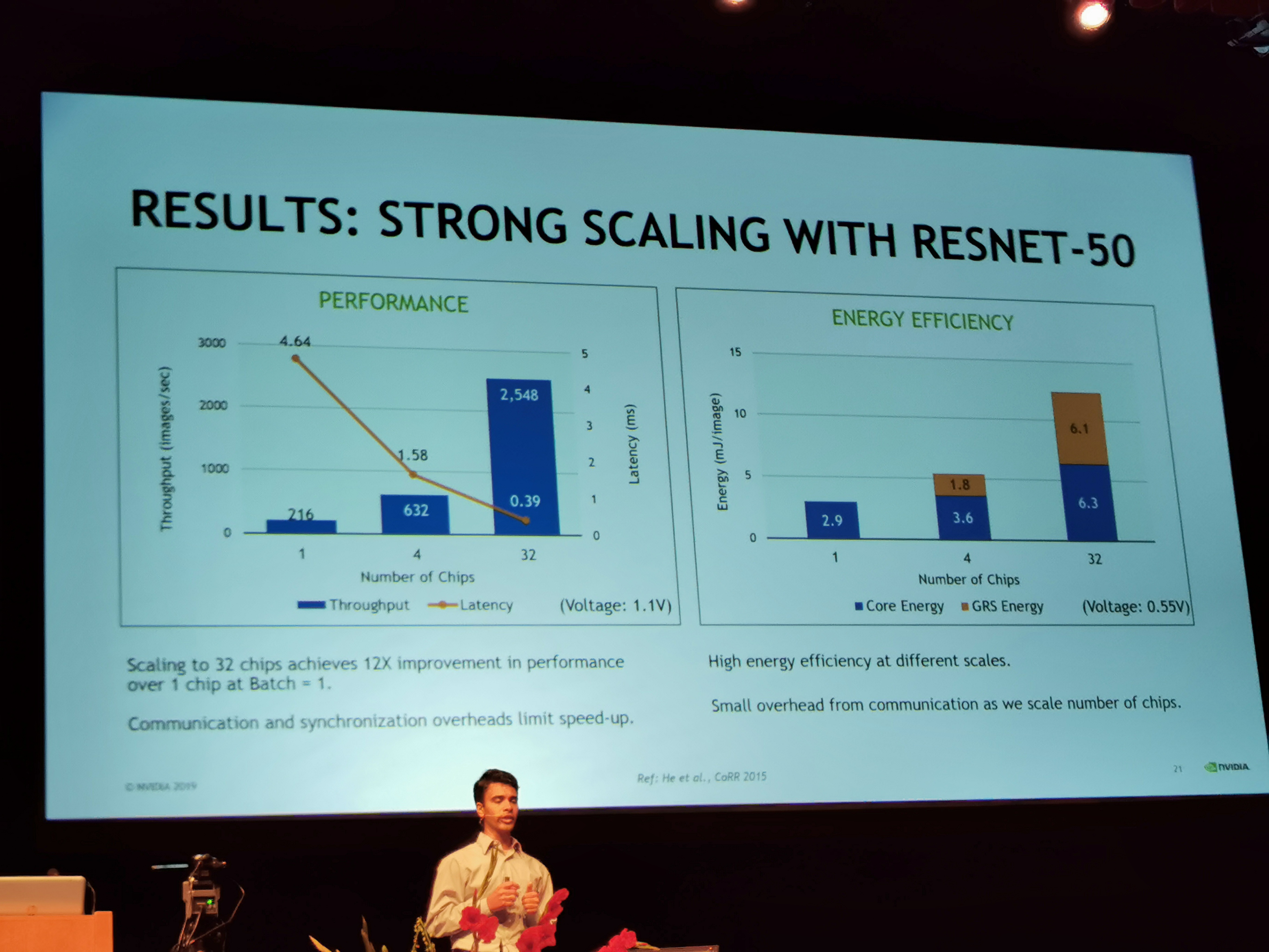
02:27PM EDT - 0.11 pJ/Op2.5K images/sec with 0.4ms latency on ResNet-50 batch = 1

02:28PM EDT - Q&A time
02:30PM EDT - Q: Results show scale 1-32 chips. Batch went up to 32 - is only one image per chip, or one image across over all chips? A: Tiling strategy depends on layer in CNN. As batch size is scaled, it gives more computations to scale to achieve better scalability. But it's not a catch-all solution.
02:32PM EDT - Q: 10 ns at 1 GHz? A: About 1.1 GHz at 0.7 volts. It includes partition interface latencies and the latency of the router itself
02:33PM EDT - Q: Physical Package? A : Organic substrate. Can be used in 2.5D
02:34PM EDT - That's a wrap. Next up is Xilinx


2 Comments
View All Comments
silencer12 - Tuesday, August 20, 2019 - link
Yeah, i am first. Look at me. Wooo(Example of all those other goofballs)
Cool article.
Rangha - Wednesday, August 21, 2019 - link
Clarification on "2:14PM EDT - PE - 8 MACs, chip is 96 MACs, package is 3456 MACs"Each Vector MAC = 8 MACs, 8 Vector MACs per PE, 16 PEs per Chip, Chip is 1024 MACs, and Package is 36864 MACs.