Intel's new Atom Microarchitecture: The Tremont Core in Lakefield
by Dr. Ian Cutress on October 24, 2019 1:30 PM EST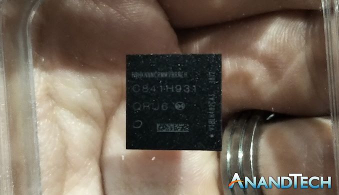
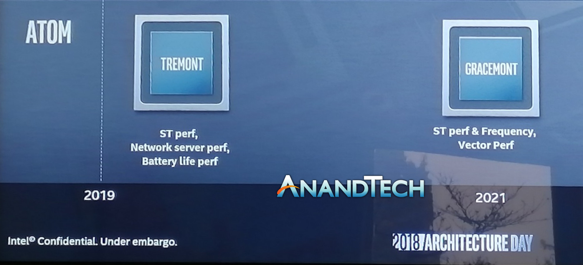
While Intel has been discussing a lot about its mainstream Core microarchitecture, it can become easy to forget that its lower power Atom designs are still prevalent in many commercial verticals. Last year at Intel’s Architecture Summit, the company unveiled an extended roadmap showing the next three generations of Atom following Goldmont Plus: Tremont, Gracemont, and ‘Future Mont’. Tremont is set to be launched this year, coming first in a low powered hybrid x86 design called Lakefield for notebooks, and using a new stacking technology called Foveros built on 10+ nm. At the Linley Processor Conference today, Intel unveiled more about the microarchitecture behind Tremont.
For the sake of clarity, a pre-note on ‘Core’ vs ‘core’:
- ‘Core’ and ‘Atom’ are Intel’s two main x86 microarchitecture families
- A ‘core’ is a single designated CPU capable of processing instructions, and can be built by Intel with either ‘Core’ or ‘Atom’ microarchitectures
A Brief History of Atom
Intel’s lower powered Atom microarchitecture has been used for a variety of solutions: embedded platforms, networking, smartphones, tablets, netbooks, NAS devices, control hubs, and a wide array of things we don’t even know about. The positioning of Atom compared to Core was meant to be that Atom was the smaller core design, taking up less silicon die area and being lower performance, but ultimately lower power in a time where the Core microarchitecture was focused more towards high performance designs.
The last few generations of Atom are readily quantified: Silvermont based on 22nm was a big product for the company, which has evolved into Airmont, Goldmont, Goldmont Plus, and now Tremont.
| Intel's Atom History | ||||||
| AnandTech | Node | Smartphone | Tablet | Netbook Notebook |
Networking Server |
|
| Saltwell | 32nm | 2011 | Medfield Clover Trail+ |
Clover Trail | Cedar Trail | |
| Silvermont | 22nm | 2013 | Merrifield Moorefield |
Bay Trail-T | Bay Trail-M Bay Trail-D |
Rangeley Avoton |
| Airmont | 14nm | 2015 | 'Riverton' | Cherry Trail-T | Braswell | Denverton |
| Goldmont | 14nm | 2016 | 'Broxton' | Willow Trail Apollo Lake |
Apollo Lake | |
| Goldmont+ | 14nm | 2017 | Gemini Lake | |||
| Tremont | 10+ | 2019 | Lakefield | Lakefield | Snow Ridge | |
The Atom family lines get a little confusing with Intel playing in all these spaces. The Atom core within in given family is usually identical (L2 configuration might change), and because of the SoC in play, it might get a different name based on the market where it was headed. Intel scrapped the smartphone program back with Broxton in 2016, and the tablet type of SoC has also gone away. With Lakefield, combining Core and Atom, it could be used in Tablets again for 2019/2020, but we will see it in Notebooks with the Surface Pro Neo and in networking/embedded markets as Snow Ridge.
Lakefield - 12mm x 12mm, 2mW Standby Power
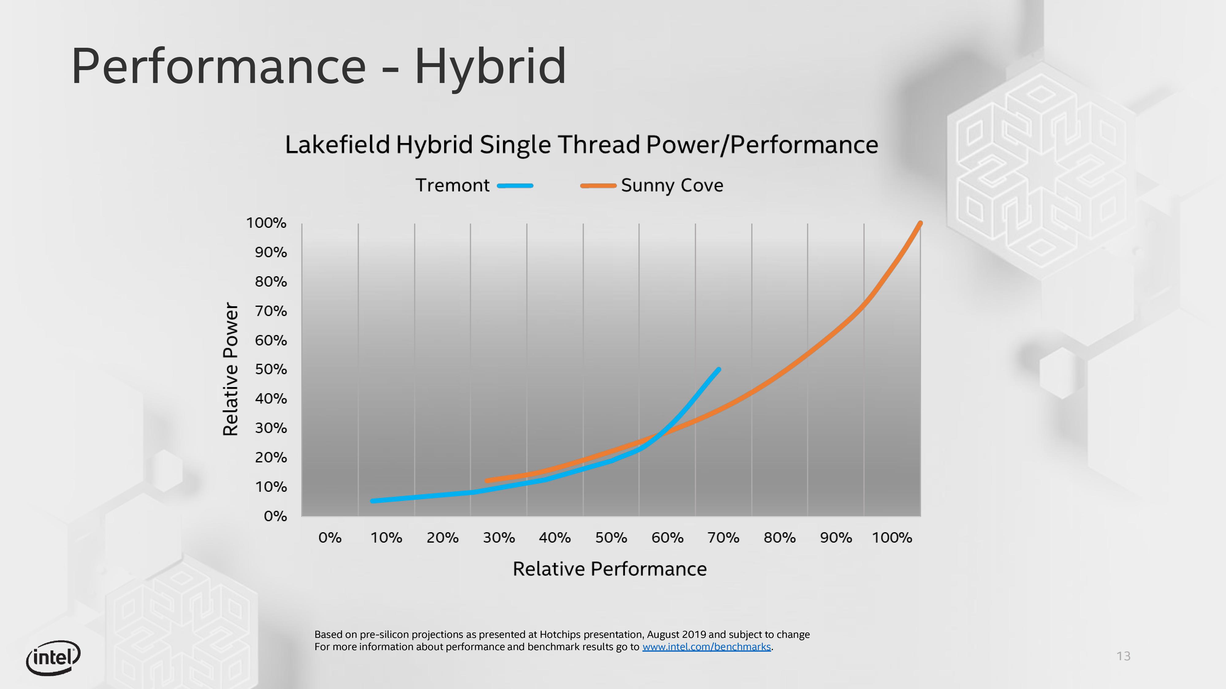
It is worth noting that as Intel expanded the scope of its Core microarchitecture, from 1.5W per core to 20W+ per core, it has kind of edged Atom more into niche products. Atom still had that super-low-power advantage, with a much smaller die area, but has also been super low performance with a quantifiable step-function below what Core can provide. With Tremont, Intel’s primary focus was bringing the single thread performance of the Atom design in parity to Core at the lower end of performance, with a sizeable overlap between the performance of a single Core design against a single Atom design. Intel published this graph to demonstrate what this looks like on early silicon:
Now, Intel’s Atom platforms haven’t had the greatest press over the last few years. Aside from providing some really nice notebooks around the $200 range on the consumer side, the enterprise side has been dealing with a clock degradation issue that ultimately leaves Atom systems built on C2000 processors unable to boot, which was bad news for embedded Atom systems designed to run for 10-20 years. Intel has since fixed that bug with a silicon update, but the point of that silicon was for it not to be touched for a generation.
With that aside, Intel is looking to revive its Atom fortunes with the new Tremont design, and looking forward to Gracemont and beyond. More performance, crossing over with Core, and with hardware built on Intel’s latest 10+ process, should afford a number of opportunities. Until we get our hands on the hardware, we’re going to examine the design.
Design Goals for Tremont
The odd quirk about CPU design is that for engineers that have been embedded in this space for 20 years, when they were taught about processor design, the main focus was all about performance. Little attention was paid to power. Fast forward to today, and power is the often talked about point when it comes to battery powered devices, and learning to design for both performance and power becomes an intense balancing act for all the engineers involved. We’ve spoken to companies that only allow performance enhancements if the power increase is at most equal in percentage, or perhaps a 2:1 ratio of performance/power. It’s a difficult pie to bake at any rate.
The interesting thing here in our briefing with Intel is that they specifically stated that Tremont was built with performance in mind, and the aim was for a sizeable uptick in the raw clock-for-clock throughput compared to the previous generation Atom, Goldmont Plus. Based on Intel’s own metrics, namely using SPEC, Intel is going to claim an average 30% iso-frequency performance uplift in core performance for Tremont over Goldmont Plus.
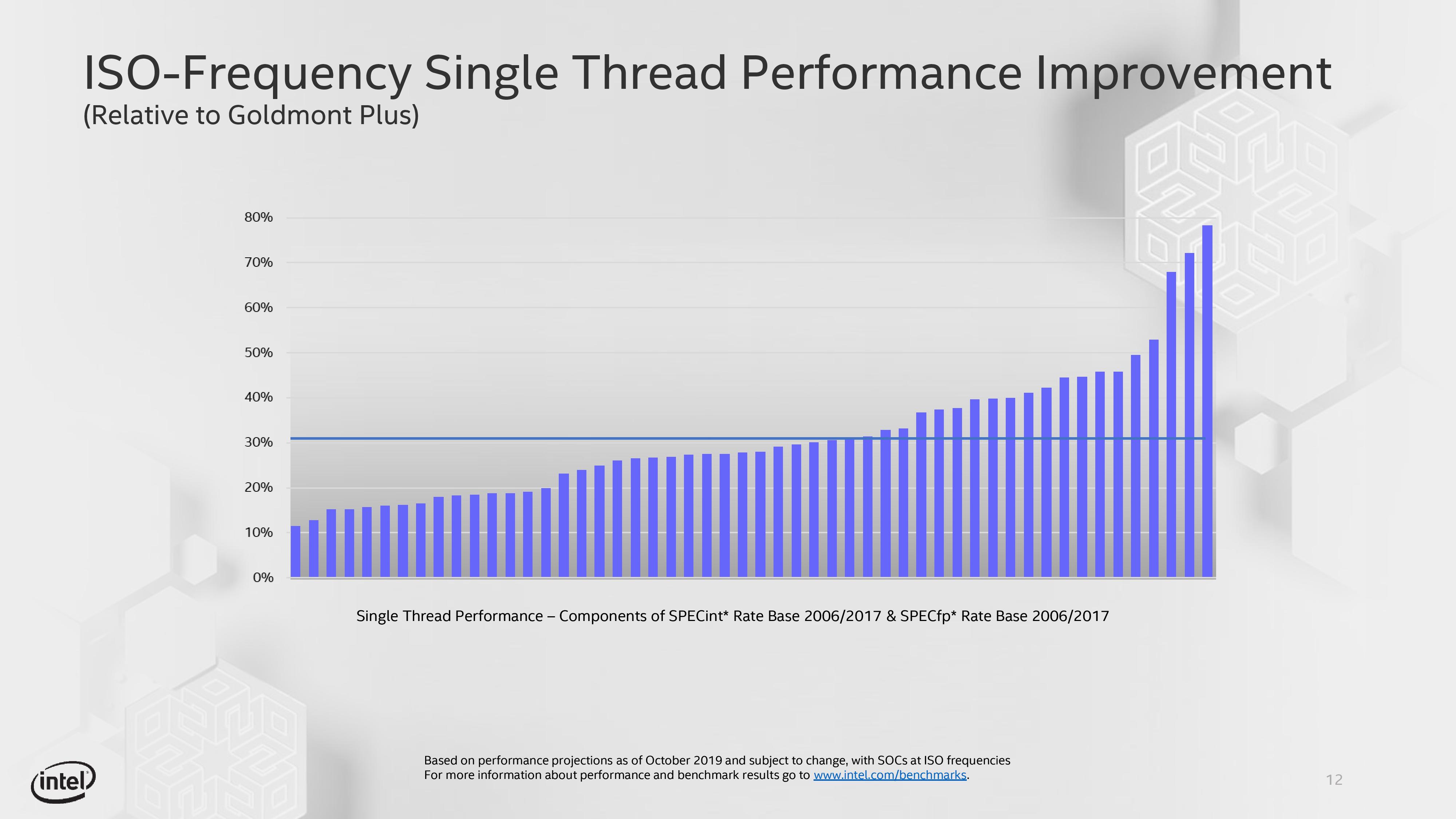
It’s worth noting here that this data is from an early Tremont design we were told, and should represent minimum uplifts. The graph is somewhat skewed at the top end with three of the SPEC tests getting 65%+ uplifts, and at the time of discussion, Intel did not have to hand exactly which tests these were (likely libquantum, lbm). We weren’t told how the code was compiled, however Intel did state that the same compiled binaries were used on both Tremont and Goldmont Plus. Intel didn’t state if they’re actually adjusting the clock of each core to match each other, or doing a performance per clock analysis using the frequency as a division factor. These results have to be taken at face value.
A 30% average jump in performance is a sizeable jump for any generation-to-generation cadence. Just taking it as-is feels premature: aside from microarchitectural advancements and a jump to 10nm, there has to be something at play here – either the power budget of Atom has ballooned, or the die area. With Intel explicitly out of the gate stating that their focusing on performance, a cynic is going to suggested that something else has paid that price, and to that end Intel wasn’t prepared to talk about power windows or die area, though they did point to the already announced Lakefield CPU, which has a 1 x Core + 4 x Tremont design and gets compared to 7 W CPUs.
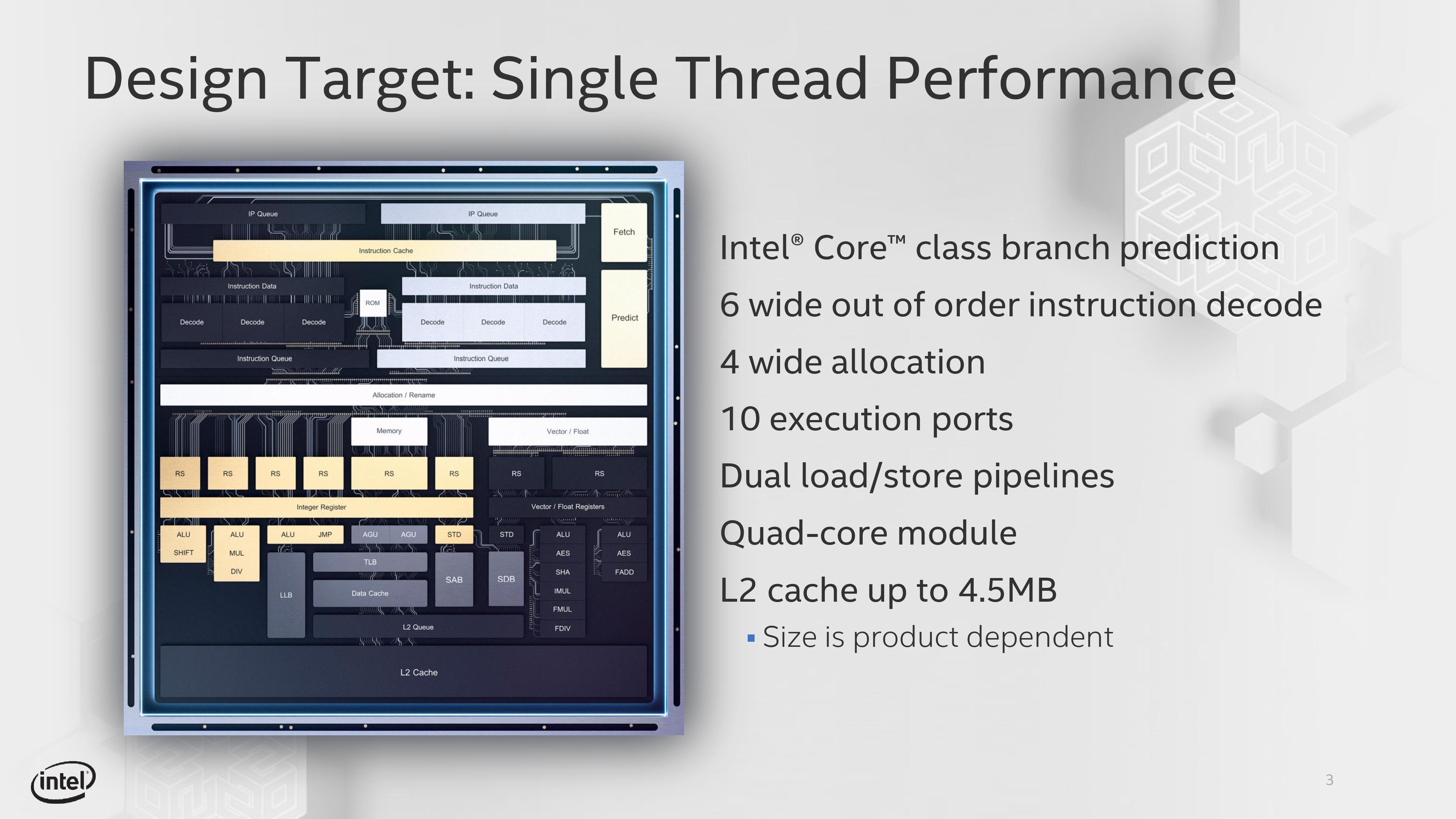
Comparing 14nm Goldmont Plus (that’s standard 14nm, not 14+ or 14++) to a 10+ Tremont core is going to be difficult: the Tremont core has more in it to drive that performance, however what is not known is how much space was saved moving from 14nm to 10+ and if the extra parts make the core bigger or smaller overall. Needless to say, Tremont has more in it to drive that performance, which we’ll cover in the next few pages.


101 Comments
View All Comments
29a - Thursday, October 24, 2019 - link
Did Atom processors ever stop sucking?solidsnake1298 - Thursday, October 24, 2019 - link
That depends on your needs. As a HTPC, starting with Apollo Lake (Goldmont) the iGPU was upgraded sufficiently that it can decode 4K HEVC. I haven't tested 4K HEVC, personally. But I have played 1080p60 HEVC without a single dropped frame.vladx - Friday, October 25, 2019 - link
I have a Goldmont tablet, 4K HEVC works fine as long as the bitrate doesn't surpass the limits of its eMMC storage, in which case artefacts and stuttering is present. Maybe I should look into replacing it with a SSD if that's even possible.qap - Friday, October 25, 2019 - link
Even the slowest eMMC storage can do 50MB/s sequential read. There is no way, you have 400Mbps+ HEVC video (and if that is the case, Atom is obviously not for you). The limit must be somewhere else. Most likely it supports hardware HEVC decoding up to some bitrate only and you are hitting this limit.vladx - Friday, October 25, 2019 - link
400Mbps no, but I have some 100+ Mbps videos and most sit around 60 so it can definitely push the eMMC to its limits especially considering it also needs to run the OS processes at the same time.s.yu - Friday, October 25, 2019 - link
A common confusion between B and b...eddman - Friday, October 25, 2019 - link
Unless the storage is so crap that can't even sustain 12.5 MB/s (a.k.a 100 Mbps), it's probably the decoder itself that is unable to properly accelerate such high bit-rate videos.nathanddrews - Sunday, October 27, 2019 - link
Quite a few eMMC implementations run off a USB 2.0 bus, so yes, it can bottleneck a system hard. Same thing frequently happens with networking components in devices. It will have AC/GbE, but can't reach those speeds.eddman - Sunday, October 27, 2019 - link
Even a USB 2.0 eMMC should be able to sustain a 12-13 MB/s sequential read.It has to be the decoder. He doesn't know the difference between bit and byte and thinks 60 Mbps is too much for 50 MB/s.
eek2121 - Monday, October 28, 2019 - link
Not if the bus is shared with 2 network controllers, a bluetooth controller, etc. I haven't looked at how Atom is set up admittedly, but that is one of the major issues with SBCs. Everything hangs off the USB 2.0 bus. The USB 2.0 bus also can't really maintain true USB 2.0 speeds in quite a few cases due to hitting micro-usb power limits.